Friday, September 26, 2014

Variable Sine Wave Oscillator Circuit

A Sine wave oscillator or a Wien bridge oscillator can be made variable by using two frequency determining parts that are varied simultaneously at high tracking accuracy.
High quality tracking potentiometers or variable capacitors are, however, expensive and difficult to obtain. To avoid having to use such a component, this oscillator was designed to operate with a single potentiometer.

The output frequency, fo, is calculated from fo = 1/(2pi.RC.rootAlpha) where R=Rz=Rz=R4=Rs, C=Ci:C2, and a=(P1+R1)R. Preset P2 allows adjusting the overall amplification such that the output signal has a reasonably stable amplitude (3.5 Vpp max.) over the entire frequency range.

The stated components allow the frequency to be adjusted between 350 Hz and 3.5 kHz. Other frequency ranges are readily defined with the aid of the above formula, although it should be noted that the upper frequency limit is determined mainly by the gain-bandwidth product of the opamps Type OP-221 and TLC272.

The current consumption of the oscillator depends on the type of opamp used. The following values were measured: OP-221: 0.5 mA; TLC272: 2mA; TLO72: 2mA. The construction of the oscillator should present very few problems since a readymade circuit board is available through our Readers Services.

Circuit diagram of a sine wave oscillator is shown below:


Precision Rectifier Circuit

This precision rectifier operates from an asymmetrical supply, handles input signals up to 3 Vpp and has a frequency range that extends from DC to about 2 kHz. Its amplification is unity, and depends mainly on the ratio R4/R3. Opamp A1 is connected as a voltage amplifier (Ao=l), Az as an inverting amplifier (Ao:-l). Opamp Az, transistor T1 and diode D2 ensure that the output voltage, U2, is identical to the positive excursions of the input voltage, U1. When U1 is positive, the out- put of A1 is held low at about 0.25 V, so that T2 is disabled and can not affect the rectified out- put signal. Components R2 and D1 protect the pnp input stage in Az against negative voltages, which are effectively limited to -0.6 V.

For negative excursions of the input signal, the function of A1, T2 and Dz is similar to the previously mentioned components. The peak output voltage . of the rectifier circuit is deter- ; mined mainly by the maximum output swing of the opamps and the voltage drop across the transistors plus D2: this amounts to about 3 V in all. When the circuit is not driven, it l consumes about lmA, and is therefore eminently suitable for building into portable, battery- operated equipment.


Mains Emergency Voltage Cut Out Circuit for Computers

 lf the voltage of the mains supply of a computer rises too high, components on the printed circuit boards can easily be damaged or even destroyed.

This emergency cutout placed between the mains supply and the load interrupts the supply when the voltage level exceeds a predetermined value. . For many reasons it is possible for the output voltage of a power supply to rise to a dangerous level. The emergency cutout described here has been set to the maximum supply voltage of 5.25 V that is stated by the manufacturers of TTL ICs. Zener diode D1 starts conducting just before the stated zener voltage is reached. A small current flows in the and gate circuit of thryristor Th1; the level of this current can be set with preset potentiometer P1 connected in parallel with the gate cathode circuit of Th1. When the mains supply rises, the current ’through the zener diode becomes large enough to cause the thyristor to fire. The firing level lies between 5.2 . . . 6 V. As soon as the thyristor fires, the mains supply voltage drops substantially because the thyristor virtually short-circuits the mains supply. ln the case of a supply without current limiting, fuse F1 prevents the current attaining too high a value.

The rating of the fuse depends, of course, on the load requirement. During testing and adjusting of the circuit, it is important that the thyristor continues to conduct after it has been fired until its current has dropped to zero. The firing voltage level can be set by means of a mains supply with a current limiter before it is put into use, lf it proves impossible, for instance because of tolerances of the zener diode, to set the firing voltage to the required value, try using a 5.1 V zener diode.

If the voltage of the mains supply of a computer rises too high, components on the printed circuit boards can easily be damaged or even destroyed. This emergency cut-out placed between the mains supply and the load interrupts the supply when the voltage level exceeds a predetermined value.

For many reasons it is possible for the output voltage of a power supply to rise to a dangerous level. The emergency cut-out described here has been set to the maximum supply voltage of 5.25 V that is stated by the manufacturers of TTL ICs. Zener diode D1 starts conducting just before the stated zener voltage is reached. A small current flows in the anode-gate circuit of thryristor Th1.

The level of this current can be set with preset potentiometer P1 connected in parallel with the gate-cathode circuit of Th1. When the mains supply rises, the current through the zener diode becomes large enough to cause the thyristor to fire. The firing level lies between 5.2 . . 6 V.

As soon as the thyristor fires, the mains supply voltage drops substantially because the thyristor virtually short-circuits the mains supply. In the case of a supply without current limiting, fuse F1 prevents the current attaining too high a value.

The rating of the fuse depends, of course, on the load requirement. During testing and adjusting of the circuit, it is important that the thyristor continues to conduct after it has been fired until its current has dropped to zero. The firing voltage level can be set by means of a mains supply with a current limiter before it is put into use. If it proves impossible, for instance because of the tolerances of the zener diode to set the firing voltage to the required value, try using a 5.1 V zener diode.
Circuit Description

Referring to the given circuit diagram of a simple DC short circuit protector for computers, the functioning may be grasped with the following points:

The zener diode along with R1 and P1 forms a voltage reference or threshold level for the thyristor gate which is connected at the the center of the above network.

P1 is adjusted to the desired threshold level at which the thyristor is required to be fired.

As long as the input voltage stays below this set level the thyristor remains inactive and the supply output to the computer undergoes a normal execution.

However if the input voltage tends to drift above the set level, the gate potential of the thyristor reaches the firing point and it fires, shorting the voltage across the output to ground.

The above action instantly drops the voltage to the safe set threshold so that now the thyristor is switched OFF.

The above triggering continues as long as the input voltage stays above the threshold mark, thus rectifying the output voltage to the safe limit, ensuring the computer a safe operating environment.


Automatic Day Night Twilight Switch Circuit

 Here is a circuit which will automaticaily light your porch light or activate any other device when the ambient light drops below a certain level.
A ·light dependent resistor is used in series with a relay. The resistor has a value in excess of ‘l megohm when illuminated, this drops A7  to below 110 ohms when day light. It is important that the LDR be positioned in such a place as not to receive any spurious illumination as this will cause the relay to drop out intermittently. A bimetallic strip type relay will give sufficient delay to ensure that incident light flashes have no influence.

Automatic Day/Night, Twilight Switch Circuit


Thursday, September 25, 2014

Digital High Low Logic Tester Circuit diagram

  1. When the input signal is logic 1, the display shows H’ and the loudspeaker emits a note which is an octave higher than the low’ tone. Operation of the circuit can be seen from the circuit diagram in figure 1 and the truth table in figure 2. When the input signal is 1, transistor T1 conducts taking the input of gate N2 above the trigger threshold and the trigger output goes to logic 0.
  2. This is not our first high and low tester, but the present circuit offers something new: a seven-segment display which shows ’H or ’L’ and at the same time a small loudspeaker emits a corresponding tone.
  3. lf required, the loudspeaker can be switched on by means of S1. The switch can, of course, be omitted if the audio tone is always required. lf you have an ear for music, R10 and R12 may be replaced by a 220 Q resistor and a 2509 preset potentiometer so that the tone can be adjusted to your particular liking.!
  4. And all that at very reasonable cost.
  5. When the supply is switched on, the decimal point of the display lights and indicates that the unit is ready For use. lf this is not the case, or an undefined signal is applied to the input, the display, apart from the decimal point, remains dark and the loudspeaker remains silent. lf the input signal is logic O, the display shows ’L’ and the loudspeaker emits a low note.
  6. When the input signal is logic 0, T1 is cut off and T2 conducts. The voltage at the inputs of gates N1 and N2 are below the trigger threshold and both outputs are logic 1, switching on transistors T3 and T4; the emitter voltage of T4 rises and cuts off diodes D4 and D5. This causes a current to flow through segments d, e and f, diodes D2 and D3, resistor R6 and transistor T3.
  7. With non-defined inputs (between 0.8.. . 2.15 V) and an open circuit input, both input transistors are cut off, The output of N1 is then logic 0 and that of N2 is logic 1: no current can therefore flow through any of the segments. As regards the drive for the two oscillators, suffice it to say that during low inputs N3 is driven by the output of N1 and during high in- puts N4 is driven directly by T1.
  8. Transistor T2 (PNP!) is cut off, the input of gate N1 is also above the trigger threshold and this trigger output is therefore also logic 0. Both switching transistors T3 and T4 are off and a current flows through the corresponding segments (b, c, e, f, g), diodes D4 and D5 and R7. 

Simple Sensitive Vibration Detector Alarm Circuit

Whether it is the hi-fi next door, the cat purring quietly, or a knock at the door, the detector described here does not miss a thing. Whenever it picks up a sound or vibration, it emits an ear-piercing tone.
The circuit is based on the use of an 8 S2 loudspeaker as microphone/ loudspeaker. As the signals from this microphone are very small, they are I amplified in A1 and rectified. The, resulting DC signal is then compared with a reference voltage in.A2. When a noise or vibration is picked up by the microphone, the voltage at the inverting input of A2 (pin 6), rises suddenly to about 4 V and then slowly decays to 0 V. The decay time depends on the time constant W R6/C3.

 The voltage at the non-inverting input of A2 (pin 5) is held constant at 0.7 V by R3/R4. When the input at pin 6 rises above 0.7 V, the output of A2 (pin 7) instantly switches to -4 V, which causes the squarewave oscillator A3 to start. The frequency (tone) of the oscillator can be adjusted by preset potentiometer Pl. The oscillator output (pin 8) is fed to amplifier stage Tl which drives the loudspeaker. The oscillator will continue to run however, so C3 charges steadily and will keep the output at pin 7 of A2 negative. As this is not the purpose of the circuit, the incoming signal must be interrupted somewhere in the chain. To do this, an FET, T2, is used as a switch. As soon as the output of the comparator becomes negative, D3 conducts, T2 is cut off and the incoming signal is interrupted. When C3 has discharged to the extent that the voltage across it drops to below 0.7 V, the output of A2 (pin 7) becomes positive, D3 is cut off and T2 conducts.

This should, however, not happen too rapidly, otherwise there is the risk that a false alarm may be given. Therefore, the gate (drive input) of T2 is connected to earth via capacitors C2 and C8. The consequent delay ensures that the circuit is not reactivated before half a second after the loudspeaker has gone quiet. The earth potential is fixed by the voltage divider R9/R10 and im- pedance converter A4, which derive a symmetrical supply of i 4.5 V from the 9 V battery. When T1 conducts, the supply voltage will drop a little because a battery cannot deliver energy as well as a mains power supply. It can therefore happen that the output signal of A3 is superimposed on the supply voltage. This undesired feed- back should be prevented by C5 and C6. lf in spite of these capacitors diffi- culties are encountered, it may be beneficial to increase the values of R5, C2 and C8 by trial and error. lf that fails to improve matters, increase the value of capacitors C5 and C6.

Indicator Circuit Diagram for Model Railway System

  1. A ninth reed contact is Htted at the end of the block, to enable turning off the indication for the relevant length of the track. The circuit is composed of 8 set-reset (S-R) bistables, which drive a LED each.
  2. This section indication system may be a just the thing you have been looking for when you own a fairly large model railway with tunnels and tracks at several levels, and are sometimes at a loss find the where abouts of a particular train.
  3. The reed contacts are actuated with the aid of a small magnet fitted to the underside of the engine. Depending on the most suitable location of the magnet, T the reed contacts are fitted in between the tracks or along- side the left or right hand rail. Several of these section indication systems may be fitted in series to enable making a con- trol panel with many lights to indicate the train positions. Observing the direction of travel of the trains, section junctions are fitted with S9 (end of previous section) and S1 (begin I of section) located next to each other.
  4. This circuit uses LEDs to indicate the train’s position. Each track block is split up into 8 sections, whose starting points are marked with reed contacts (Si-S8).
  5. All SET inputs are combined in a NOR gate, N1, which drives a pulse shaper and buffer to reset the bistables with a brief pulse to ensure that only the LED for the last passed track section is lit. 
Indicator circuit for model railway


Making PCB at Home

Making
The heart of any electronic project is the PCB. Without a proper PCB, a project may end up in total failure.
A perfect PCB · gives a face lift to the appearance and performance of the circuit and, what is of greater importance, its neatness facilitates easy troubleshooting. As soon as a project is taken up, the first thing that comes to the mind is a ready made PCB. When it is not avail- able, the universal veroboard (VB) is substituted by many hobbyists and some professionals too! An easy way to make 1 a PCB is described here.


Materials required
1. Hand drill
2. Electric drill
‘ 3. Drill bits 0.8 mm and 3 mm
4. Minor hacksaw
5. Rat tail file
6. Clamp
7. Enamel paint (can be left out if
PCB pen is available)
8. Fine painting brush (pointed tip)
(can be left out if PCB pen is available)
9. Ferric chloride
10. Veroboard (VB) with 0.1 inch
spaced array of holes
11. Copper clad board (CCB)
12. Transparent foot rule.

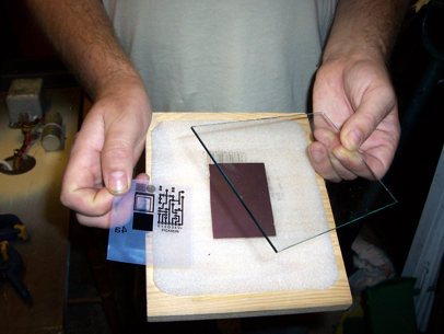
Gather all the components needed for the project. In the case of  ICs, use IC base for all. Bend the leads of all the components according to their sizes and mount them on the VB, as far as possible, in identical position as in the circuit. Remember to leave enough space around each component, for the copper tracks pass around them in parallel fashion on the other side of the board. Give serious consideration to this point when there are ICs. In short, spread out the components. The holes through which the leads of the components are protruding should be marked using an ordinary pencil (which can be rubbed off or erased after finishing the PCB project). The above procedure determines the size of the copper clad board (CCB) required for the project. CCB of the required size can be purchased or cut off from a bigger piece. The vertical and horizontal centre lines separating the CCB into four segments may be drawn on the copper foil using the transparent foot rule and a sharp needle applying light pressure.

Place the VB on theCCB such that thc copper foil on thc CCB and the pencil markings on the VB are facing up. The CCB must .be adjusted to be exactly at the centre of the layout on the VB. This can be achieved by looking through the VB matrix to locate the centre lines drawn on the copper foil of the CCB. The board pair can then be placed on a wooden plank and the clamp may be used to secure them tight before drilling. A more sophisticated clamp can be used after gaining some experience with this small gadget.  

Electric PCB drilling machines are quite expensive. A manually operated drill would suffice for an electronics hobbyist. But for people who want to make this job less tiresome, here is a simple way to make a PCB driller. The normal sewing machine motor or a similar high RPM motor with a regulator foot control is ideal. Remove the V- belt, clamps and pulley. Procure a double  end jaw mouth from a watch repair shop and cut exactly at the centre, using a hacksaw. Attach one end of the jaw to the shaft of the motor. A careful scrutiny of the motor and the jaw mouth is required to get the drill bit exactly at the centre. This device can take up drilling of 0.8mm holes for ICs at precise dimensions and spacings.

Hold the motor of the above device (or hand drill) and start drilling. The drill must never be allowed to rest on the drill bit as it will definitely snap under pressure. Drill the CCB through the VB at all the pencil markings made on the VB. A few minutes of practice would give an idea about the amount of control needed on the foot regulator and also the extent of pressure to be allowed to rest on the drill bit, while the shaft is revolving at high speed. To avoid waste material or debris coming out of the CCB through the VB holes, a half depth drill on PCB may be made throughout and later drilled to the full depth without the VB. This will prolong the life of the VB without damaging its holes and also save the trouble of blowing out the debris at short intervals while looking for pencil markings.

 When the drilling is complete, try to imagine the circuit on a paper as it should appear on the copper side. Trial tracks may be drawn using a pencil from one hole to the other. The most efficient, shortest possible layout with least likely interference due to inter- track capacitance, induction, etc may be arrived at. The tracks should not have sharp corners and must be wide enough for the current they carry.

 It is highly probable that while trying out the circuit, two separate tracks may cross one another without any short between the two. This can be avoided by the use of jumpers (wires placed on the component side of the board). The l position of the holes for the jumpers- may be placed conveniently on the copper side without trespassing into another component on the component side. The position of these holes must be made stable for the drill bit by ‘centre punching’, using the sharp tip of the rat tail file. Never try drilling the CCB without  the punch mark because in the absence of the VB, the drill bit has the tendency to drift fast and break as soon as the regulator is pressed. The copper foil may also get damaged by the drifting drill bit.

The jumpers must be parallel and non-overlapping to facilitate assembly. When there are too many jumpers, as in the cmse of multi-lead components like microprocessor ICs, double sided PCBs are the only solution.

Holes must be drilled along one or more edges according to the require- ments and convenience for power sup- ply, input, output and interstage connections, if any. For securing the PCB on any cabinet, use 3mm drill bit at convenient points on the CCB, usually the four corners.

Instead of a PCB pen, a fine tipped brush is used to apply a thin coat of enamel paint lines on the pencil tracks to complete the circuit. A small blob of paint may be applied to each drill hole so that the etchant does not eat away the copper at the crucial soldering points. This blob gives the advantage of producing a perfect circular copper terminus on each hole. If a track is wrongly drawn with paint, it is better to leave it y there to dry up and then remove it using a razor blade or knife. Wet paint, when removed using a cloth, leaves behind a thin transparent coat of the enamel which prevents etching at that point. The paint should not be allowed to dry up completely as it becomes very difficult to remove it after the etching process. The unused portion of the copper on the CCB may be painted without touching other tracks and connected to the main ground. Conditions like interference, ground loop, etc should be considered before finishing the painting work.

he CCB with half dried paint immersed in a solution of ferric chloride (containing a few drops of concentrated hydrochloric acid to prevent precipitation of ferric hydroxide). A plastic tray, porcelain or glass plate would be ideal for storing the solutions. Depending on the concentration of the etchant, etching time may vary. When etching is over, the paint should be wiped off with a cloth dipped in kerosene. Hard dried paint may be removed by using acetone. The drill may again be used to clean the holes which may have been clogged by the paint. Soon after etching and cleaning, soldering of the components should be taken up. If this is delayed, oxidation of the copper film may lead to difficulty in Soldering.

Simple Frequency Doubler Circuit

This is a simple three transistor frequency doubler circuit to raise an audio frequency by a factor of two i.e., one octave.
O1 is connected as a phase splitter with anti-phase signals·’ appearing at its collector and emitter. These signals are fed to two emitter followers Q2 and O3, which have a common emitter resistor, and thus add the two anti-phase signals. A degree of distortion is inevitable as shown in Fig. 2, but is acceptable for speech and soloists and produces a sound similar to the Chipmunks or Pinky and Perky. 


Wednesday, September 24, 2014

Simple Light Activated Alarm Circuit

  1. Working of second and third sections is known to many of the hobbyists- second is merely a multivibrator, `whereas third is an audio amplifier.
  2. This device comprises a triggering section, an oscillating section, and an amplification section.
  3. SCR] may be triggered either by bringing the gate of SCRI in contact with positive pole of the battery momentarily or by flashing a light on the light dependent resistor (LDR).
  4. By adjusting potentiometer. VRI, the sensitivity of the instrument can be controlled. To switch off the alarm the battery will have to be disconnected momentarily.
  5. This signal is amplified by the third section and produces an audio alarm through the speaker. This circuit works on 9V.
  6. Even a light from a cigar can trigger the silicon controlled rectifier. On power (negative voltage) being applied, the second section produces oscillations.
  7. When light falls on the LDR, its resistance is reduced, thereby a current flows through the gate of SCR]. This gate current triggers SCR] and the oscillating and amplification sections of the alarm get negative voltage.
  8. These two sections commonly get negative voltage when SCRI is triggered. 

AC Mains Lamp Flasher Circuit Diagram

This electric lamp flasher which may be used as a warning light works directly on 230V-AC mains. - The diodes Dl to D4 in convert the alternating voltage into pulsating DC voltage. Components Rl, Cl, R2 and C2 form the timing circuit to control the flashing rate.  When the charged voltage across the capacitor C2 exceeds the neon’s (Nl) firing voltage, the neon fires and provides the  required triggering current to SCR. Then the SCR also fires and acts as a short, connecting the lamp across the AC mains. Finally, when the voltage across capacitor C2 falls below the maintaining voltage of the neon, the neon stops conducting and the SCR also returns to its non-conducting state, thus disconnecting the lamp from AC mains. The capacitor C2 starts charging again and the cycle repeats.

The lamp flashes in this circuit once every second. The rate can be varied, if required, by adjusting R2. The circuit of Fig. 2 is a simpler and a more economical arrangement. lt uses only one diode instead of four for rectification. ln fact, an SCR itself is a rectifier and power halving is done by it. The diode Dl is however required because without it the timing period will get disturbed during negative cycles. Incidentally, it helps to increase the reverse voltage ratings of the SCR and also protects the electrolytic capacitors by providing a proper polarity voltage. ln this arrangement the lamp flashes at a reduced brightness. Thus the circuit acts as a lamp flasher-cum-wattage halver.

 A 100W bulb used in this circuit, acts as a 50W lamp flasher. The lamp flasher may be light-controlled by adding an LDR across the timing capacitor C2. An LDR has high resistance in darkness and has little effect on the circuit functioning. When light falls on it (during day time), its resistance becomes sufficiently low to prevent the capacitor from charging to the neon lamp firing voltage. Instead of LDR a simple switch or reed relay contacts can also be used to short-circuit the capacitor C2 when the flasher is not required. Thus, by controlling low current path of triggering circuit, the high load current of the lamp can be switched on and off very conveniently. Caution: Since the flasher uses a SCR, RF interference can be a problem. lt is therefore advised to use a filter for eliminating the interference. 


Simple 100 watt Inverter Citcuit Using IC 4049

You should not install the transistors straight onto the heat sinks. Make use of mica isolation kit to prevent immediate exposure and short circuiting of the transistors together as well as the ground.
Clamp the heat sink set up to the of a nicely ventilated, durable, heavy gauge metal enclosure.
Additionally attach the power transformer beside the heat sinks employing nuts and bolts.
Now attach the suitable areas of the constructed circuit board to the power transistors on the heat sinks.
Lastly connect the power transistor’s outputs to the supplementary winding of the power transformer.
Complete the building by fixing and interconnecting the exterior electrical “fittings” such as fuses, sockets, buttons, mains cord along with the battery inputs.
An alternative individual power source circuit using a 12V/3Amp. transformer might be included inside to recharge the battery the moment needed (see diagram).


You may further discover how to construct a simple 100 watt inverter circuit by focusing on the following examination method:


To better know how to construct an inverter, you will need to find out how the circuit features by means of nthe following actions:
Gates N1 and N2 of IC 4049 are configured as an oscillator. It carries out the major operation of providing square waves to the inverter part.
Gates N3... N6 are utilized as buffers to ensure that the circuit is not load dependant.
Alternating voltage from the buffer phase is applied to the base of the current amplifier transistors T1 and T2. These particular transistors execute in line with the applied alternating voltage and amplifies it to the base of the output transistors T3 and T4.

All these output power transistors oscillate at a complete swing, dispensing the full battery voltage into the every half of the secondary winding alternately.

This secondary voltage is brought on in the main winding of the transformer which is stepped-up into an effective 230 volts (AC). This voltage is employed to power the output load.
Testing Procedure

You can further understand how to build an inverter by focusing on the following testing procedure given in a comprehensive manner below:


Start out the testing method by attaching a 1 hundred watt bulb at the output socket of the inverter,

Add a 15 Amp./12V fuse inside the fuse holder,

At last connect a 12V car or truck battery to the battery inputs of the inverter.

If all the contacts are proper, the 100 Watt bulb must right away light brightly.

Continue the inverter ON for 60 minutes and let the battery discharge through the bulb,

Then transfer the given toggle switch to the charging mode, verify the meter reading,

The meter need to suggest the charging current of the battery.

The digital meter reading should certainly slowly die down to nil after a period of time, making sure that the battery is entirely charged and geared toward the subsequent action.

Capacitive Switch Circuit Diagram

  1. The 555 or 7555 timers will oscillate in a stable manner.
  2. However, if we add an external capacitive sensor it becomes possible to vary the oscillation frequency. In this circuit the square wave is integrated by the triple RC network, while lC2, used as a comparator (with a variable reference value), uses the changes in the integrated voltage to alternately make and break the relay. Thus when you move close to C the relay makes; if you remain stationary the relay breaks.
  3. By changing the existing frequency of the signal the average integrated value remains the same but, at the instant when the frequency is changed, a positive or negative voltage peak will appear due to the momentary change in the average waveform of the signal.
  4. Failing this the operation of the circuit would often be disrupted by false detections. Coarse l and fine adjustment is provided, using P1 and P2, to reduce the risk of incorrect switching. Note: The numbers in parentheses are the pins if an LM3l1 is used in place of the CA3130.
  5. Without this refinement the size of the sensitive plate must be such that the frequency of oscillation be at least , several kHz.
  6. It may seem a bit basic but it is a valid idea and it is worth ) looking at it in greater detail.
  7. Take a square wave signal with a given frequency and integrate it. This gives a stable continuous average voltage.
  8. To obtain better results you could take the signal after integration and differentiate between negative pulses (the frequency decreases as the value of C increases: when the sensor is approached) and positive pulses (the frequency increases again if the sensor is no longer affected) and compare them.
  9. This is the principle upon which our switch is based. 
Capacitive Switch Circuit Diagram

Tuesday, September 23, 2014

22 Watts Mini Subwoofer Circuit TDA1516 with Adjustable Frequency

The subwoofer is a subwoofer or a speaker to reproduce low frequencies, devotee of 20 Hz to 150 Hz electronic circuit diagram below shows the details of a scheme of the main amplifier TDA1516 22 watt in 4 ohm car subwoofer driver. This device is designed for an existing stereo amplifier, often requires adding another blow to the music of driving a subwoofer.

The amplifier uses BTL is a good and cheap ((Bridge Tied Load channels) 13-pin IC TDA1516 from Philips is now NXP Semiconductors), which may provide a small number of components and 22W at 4 ohm load voltage 12 volt car battery default.

The device consists of several parts: the name of the potentiometer, dual-linear motion potentiometers, 1/4W resistors, capacitors, electrolytic 25V, 63V Polyester capacitors, LED, 100 mA NPN transistor, dual BIFET Op-Amp, 24 W BTL car radio RCA audio input amplifier and two speakers 4 ohm or 8 ohm woofers in isobaric parallel wiring.


DIY 12 volt car project Subwoofer frequency low-pass filter circuit and BTL Amplifier TDA1516

The signals from the line outputs for stereo mixing amplifier input drive, and taking into account the level of the signal to the buffer and can be reversed IC1A phase SW1. Such control may be useful to the subwoofer in phase with the speaker of the existing car radio.

Then, a variable frequency 12dB/octave-pass low IC1B, the components of the Q1 and then you can pass the low frequency of 70 Hz or 150 Q2, R17 and C9 form a voltage stabilizer to facilitate access and filtering circuit to prevent track of the services given power at a low level positive.

LPF subwoofer and amplifier parts list:


Potentiometer
P1-10K
P2-22K

Resistor
R1, R4-1K
R2, R3, R5, R6-10K
R7, R8-100K
R9, R10, R13-47K
R11, R12-15K
R14, R15, R17-47K
R16 6K8
R18-1K5

Capacitor
C1, C2, C3, C6-4μ7 25V
C4, C5-68NF 63V
C7 33nF 63V
C8, C9 220μF 25V
C10 470nF 63V
C11 100nF 63V
C12 2200uF 25V

Diode
D1 LED Lamp

Transistor
Q1, Q2 BC547

IC
IC1-TL072 Op-Amp
IC2-TDA1516BQ Car Amplifier 24 Watt BTL

Switch
SW1-Toggle SPDT
SW2-Toggle SPDT

RCA Jack
J1, J2 RCA Audio Input

SubWoofer Drive Unit
4-ohm woofer driver or two 8 ohm woofers connected to Isobaric 

One Transistor FM Radio Receiver Circuit

Here’s simple FM receiver circuit for a simple superregenerative FM radio. It is sensitive, selective, and has enough audio drive for an earphone. These designs generally have low component counts, however the design or my construction have been far from simple.

FM Receiver Schematic

FM Radio Receiver Circuit Layout
Because this is a superregenerative design, component layout can be very important. The tuning capacitor, C3, has three leads. Only the outer two leads are used; the middle lead of C3 is not connected. Arrange L1 fairly close to C3, but keep it away from where your hand will be. If your hand is too close to L1 while you tune the radio, it will make tuning very difficult.

Winding L1
L1 sets the frequency of the radio, acts as the antenna, and is the primary adjustment for super-regeneration. Although it has many important jobs, it is easy to construct. Get any cylindrical object that is just under 1/2 inch (13 mm) in diameter. I used a thick pencil from my son’s grade school class, but a magic marker or large drill bit work just fine. #20 bare solid wire works the best, but any wire that holds its shape will do. Wind 6 turns tightly, side-by-side, on the cylinder, then slip the wire off. Spread the windings apart from each other so the whole coil is just under an inch (2.5 cm) long. Find the midpoint and solder a small wire for C2 there. Mount the ends of the wire on your circuit board keeping some clearance between the coil and the circuit board.

A tuning knob for C3

C3 does not come with a knob and I have not found a source. A knob is important to keep your hand away from the capacitor and coil when you tune in stations. The solution is to use a #4 nylon screw. Twist the nylon screw into the threads of the C3 tuning handle. The #4 screw is the wrong thread pitch and will jam (bind) in the threads. This is what you want to happen. Tighten the screw just enough so it stays put as you tune the capacitor. The resulting arrangement works quite well.

FM Radio Receiver Circuit Adjustment
If the radio is wired correctly, there are three possible things you can hear when you turn it on: 1) a radio station, 2) a rushing noise, 3) a squeal, and 4) nothing. If you got a radio station, you are in good shape. Use another FM radio to see where you are on the FM band. You can change the tuning range of C3 by squeezing L1 or change C1. If you hear a rushing noise, you will probably be able to tune in a station.

Try the tuning control and see what you get. If you hear a squeal or hear nothing, then the circuit is oscillating too little or too much. Try spreading or compressing L1. Double check your connections. If you don’t make any progress, then you need to change R4. Replace R4 with a 20K or larger potentiometer (up to 50K). A trimmer potentiometer is best. Adjust R4 until you can reliably tune in stations. Once the circuit is working, you can remove the potentiometer, measure its value, and replace it with a fixed resistor. Some people might want to build the set from the start with a trimmer potentiometer in place (e.g., Mouser 569-72PM-25K).

BA1404 HI FI Stereo FM Transmitter Kit circuit


Be "On Air" with your own radio station! BA1404 based transmitter is an exciting product that will broadcast high quality stereo signal in 88MHz - 108MHz FM band. It can be connected to any type of stereo audio source such as iPod, Computer, Laptop, CD Player, Walkman, Television, Satellite Receiver, Tape Deck or other stereo system to transmit stereo sound with excellent clarity throughout your home, office, yard or camp ground. Add our 500mW FM / VHF Transmitter Amplifier / Booster for even longer range.

The circuit is based on the popular BA1404 stereo broadcaster IC which contains all the complex circuitry for generating the stereo FM signal. 38 KHz crystal provides a rock solid stability of sub-carrier for stereo signal. PCB includes green solder mask layer for easier soldering and protects wires that do not need soldering.

Kit Components
1x Printed Circuit Board [5 cm x 3.2 cm]
1x BA1404 Stereo FM Transmitter IC
1x 38KHz Crystal Oscillator
1x 3.5T Variable Precision RF Coil
1x 10uH Inductor
4x 10uF/35V Capacitor
4x 1nF Ceramic Capacitor
2x 1nF Mylar Capacitor
1x 220pF Ceramic Capacitor
5x 10pF Ceramic Capacitor
2x 47K Resistor
2x 27K Resistor
1x 150K Resistor
1x 5.6K Resistor
1x 270 Resistor
1x Instructions

10 Amp 13 8 Volt Power Supply description and circuit diagram

Sometimes amateurs like to home-brew their power supplies instead of purchasing one off the shelf at any of the major ham radio retail dealers. The advantage to rolling your own power supply is that it teaches us how they work and makes it easier to troubleshoot and repair other power supply units in the shack. It should be noted that there is no real cost advantage to building your own power supply unless you can get a large power transformer and heat sink for a super low price. Of course rolling our own gives us the ability to customize the circuit and make it even more reliable than commercial units.

The circuit in Figure 1 will give us 10 amps (12 amps surge) with performance that equals or exceeds any commercial unit. The circuit even has a current limiting feature which is a more reliable system than most commercial units have. Just like other commercial units, this circuit uses the LM723 IC which gives us excellent voltage regulation. The circuit uses 3 pass transistors which must be heat sinked. Resistor R9 allows the fine tuning of the voltage to exactly 13.8 volts and the resistor network formed by resistors R4 through R7 controls the current limiting. The LM723 limits the current when the voltage drop across R5 approaches .7 volts. To reduce costs, most commercial units rely on the HFE of the pass transistors to determine the current limiting. The fault in that system is that the HFE of the pass transistors actually increases when the transistors heat up and risks a thermal runaway condition causing a possible failure of the pass transistors. Because this circuit samples the collector current of the pass transistors, thermal runaway is not a problem in this circuit making it a much more reliable power supply. The only adjustment required is setting R9 to the desired output voltage of anywhere between 10 and 14 volts. You may use a front panel mounted 1K potentiometer for this purpose if desired. Resistor R1 only enhances temperature stability and can be eliminated if desired by connecting pins 5 and 6 of IC-1 together. Although it really isn’t needed due to the type of current limiting circuit used, over voltage protection can be added to the circuit by connecting the circuit of Figure 2 to Vout. The only way over voltage could occur is if transistors Q2 or Q3 were to fail with a collector to emitter short. Although collector to emitter shorts do happen, it is more much more likely that the transistors will open up when they fail.

Circuit diagram

I actually tested this and purposely destroyed several 2N3055’s by shorting the emitters to ground. In all cases the transistors opened up and no collector to emitter short occurred in any transistor. In any event, the optional circuit in Figure 2 will give you that extra peace of mind when a very expensive radio is used with the power supply. The circuit in Figure 2 senses when the voltage exceeds 15 volts and causes the zener diode to conduct. When the zener diode conducts, the gate of the SCR is turned on and causes the SCR to short which blows the 15 amp fuse and shuts off the output voltage. A 2N6399 (Tech America) was used for the SCR in the prototype but any suitable SCR can be used. While over voltage protection is a good idea, it should not be considered a substitute for large heat sinks. I personally feel the best protection from over voltage is the use of large heat sinks and a reliable current limiting circuit. Be sure to use large heat sinks along with heat sink grease for the 2N3055 transistors. I have used this power supply in my shack for several months on all kinds of transceivers from HF, VHF to UHF with excellent results and absolutely no hum. This power supply will be a welcome addition to your shack and will greatly enhance your knowledge of power supplies.

DE N1HFX

Parts
R1 1.5K ¼ Watt Resistor (optional, tie pins 6 & 5 of IC1 together if not used.)
R2,R3 0.1 Ohm 10 Watt Resistor (Tech America 900-1002)
R4 270 Ohm ¼ Watt Resistor
R5 680 Ohm ¼ Watt Resistor
R6,R7 0.15 Ohm 10 Watt Resistor (Tech America 900-1006)
R8 2.7K ¼ Watt Resistor
R9 1K Trimmer Potentiometer (RS271-280)
R10 3.3K ¼ Watt Resistor
C1,C2,C3,C4 4700 Microfarad Electrolytic Capacitor 35 Volt (observe polarity)
C5 100 Picofarad Ceramic Disk Capacitor
C6 1000 Microfarad Electrolytic Capacitor 25 Volt (observe polarity)
IC1 LM723 (RS276-1740) Voltage Regulator IC. Socket is recommended.
Q1 TIP3055T (RS276-2020) NPN Transistor (TO-220 Heat Sink Required)
Q2,Q3 2N3055 (RS276-2041) NPN Transistor (Large TO-3 Heat Sink Required)
S1 Any SPST Toggle Switch
F1 3 Amp Fast Blow Fuse
D1-D4 Full Wave Bridge Rectifier (RS276-1185)
T1 18 Volt, 10 Amp Transformer Hammond #165S18 (Tech America 900-5825)


author: N1HFX
e-mail:
web site: http://www.electronics-lab.com

Monday, September 22, 2014

Class A Power Amp mosfet

https://blogger.googleusercontent.com/img/b/R29vZ2xl/AVvXsEiflhTGWBJ0mAR_njRS4p6i6UMkE7RVcRJjAbK4KQtFeDjSIKqrk91kcKqLIOXbWXqD2XMf4ZCt53QMUX_Hs5pR1Sd375qIeTuzN1dRQO-ax07VmckiN2F0jeu69imL8hUncXcV8mJv5p2J/s400/Class+A+MOSFET+Amplifier+2SK1058.png

A power MOSFET is biased using a pot (needed to correct for different device characteristics) so that the voltage at the drain is about 1/2 the supply voltage. Current is limited using a constant current source, and this needs to be set to provide a current that is higher than the maximum peak current to the speaker. Since the amp is not DC coupled, an output capacitor is needed to keep the DC out of the loudspeakers. An input cap is also needed to stop the source (the preamp, or for my tests, an audio oscillator) from stealing the bias voltage.

Read More original Source:
http://www.sound.westhost.com/project36.htm

Basic UPS Power Supply circuit and Description

Description

This circuit is a simple form of the commercial UPS, the circuit provides a constant regulated 5 Volt output and an unregulated 12 Volt supply. In the event of electrical supply line failure the battery takes over, with no spikes on the regulated supply.

Circuit diagram

Notes:
This circuit can be adapted for other regulated and unregulated voltages by using different regulators and batteries. For a 15 Volt regulated supply use two 12 Volt batteries in series and a 7815 regulator. There is a lot of flexibility in this circuit.
TR1 has a primary matched to the local electrical supply which is 240 Volts in the UK. The secondary winding should be rated at least 12 Volts at 2 amp, but can be higher, for example 15 Volts. FS1 is a slow blow type and protects against short circuits on the output, or indeed a faulty cell in a rechargeable battery. LED 1 will light ONLY when the electricity supply is present, with a power failure the LED will go out and output voltage is maintained by the battery. The circuit below simulates a working circuit with mains power applied:

Between terminals VP1 and VP3 the nominal unregulated supply is available and a 5 Volt regulated supply between VP1 and VP2. Resistor R1 and D1 are the charging path for battery B1. D1 and D3 prevent LED1 being illuminated under power fail conditions. The battery is designed to be trickle charged, charging current defined as :-
(VP5 - 0.6 ) / R1
where VP5 is the unregulated DC power supply voltage.
D2 must be included in the circuit, without D2 the battery would charge from the full supply voltage without current limit, which would cause damage and overheating of some rechargeable batteries. An electrical power outage is simulated below:

Note that in all cases the 5 Volt regulated supply is maintained constantly, whilst the unregulated supply will vary a few volts.

Standby Capacity
The ability to maintain the regulated supply with no electrical supply depends on the load taken from the UPS and also the Ampere hour capacity of the battery. If you were using a 7A/h 12 Volt battery and load from the 5 Volt regulator was 0.5 Amp (and no load from the unregulated supply) then the regulated supply would be maintained for around 14 hours. Greater A/h capacity batteries would provide a longer standby time, and vice versa.


author: Andy Collinson
e-mail: anc@mitedu.freeserve.co.uk
web site: http://www.zen22142.zen.co.uk

Sunday, September 21, 2014

220 Volts Flashing Lamps

Especially designed for Christmas tree lamps Replaces old thermally-activated switches This circuit is intended as a reliable replacement to thermally-activated switches used for Christmas tree lamp-flashing. The device formed by Q1, Q2 and related resistors triggers the SCR. Timing is provided by R1,R2 & C1. To change flashing frequency dont modify R1 and R2 values: set C1 value from 100 to 2200µF instead. Circuit diagram : 220 Volts Flashing Lamps Circuit Diagram Best performances are obtained with C1=470 or 1000µF and R4=12K or 10K. Due to low consumption of normal 10 or 20 lamp series-loops intended for Christmas trees (60mA @ 220V typical for a 20 lamp series-loop), very small and cheap SCR devices can be used, e.g. C106D1 (400V 3.2A) or TICP106D (400V 2A), this last and the suggested P0102D devices having TO92 case.

Parts List:

R1 100K 1/4W Resistor
R2,R5 1K 1/4W Resistors
R3,R6 470R 1/4W Resistors
R4 12K 1/4W Resistor
C1 1000µF 25V Electrolytic Capacitor
D1-D4 1N4007 1000V 1A Diodes
D5 P0102D 400V 800mA SCR
Q1 BC327 45V 800mA PNP Transistor
Q2 BC337 45V 800mA NPN Transistor
PL1 Male Mains plug
SK1 Female Mains socket

Note: For proper operation its absolutely necessary to employ high Gate-sensitive SCRs. If you are unable to find these devices you can use Triacs instead. In this case the circuit operates also with relatively powerful devices. A recommended Triac type is the ubiquitous TIC206M (600V 4A) but many others can work.Note that in spite of the Triac, diode bridge D1-D4 is in any case necessary.

This circuit was awarded with publication in ELECTRONICS WORLD "Circuit Ideas", June 2000 issue, page 458

Fuse Box BMW 328i 1999 Engine Compartment Diagram

Fuse Box BMW 328i 1999 Engine Compartment Diagram - Here are new post for Fuse Box BMW 328i 1999 Engine Compartment Diagram.

Fuse Box BMW 328i 1999 Engine Compartment Diagram


Fuse
Fuse

Fuse Panel Layout Diagram Parts: inside mirror electrochromic, interior light, light module, make up mirror light, navigation, on board computer, outside mirror, parking aid, passenger compartment, radio, rain sensor, rear wiper, roler sun blind, secondary air pump, side airbag, socket, speed control, starter interlock, telephone, trailer coupling, window lift, windscreen washer.

Amplifier current negative feedback TDA7294 DC Servo

TDA7294

In the field of consumer reports electronics products reviews, product size, weight is toward smaller, lighter direction, high-power single-chip audio power amplifier needs of increasingly prominent, TDA7294 is currently the best performance, the biggest single-chip audio power amplifier One.

It consists of the European SGS-THOMSON Italian-French company in accordance with discrete components A and B audio amplifier circuit design from classic. Its former low-level noise, low distortion of the bipolar transistor circuit, at the end of a high-pressure, high current DMOS output of the buffer, it has bipolar circuit sounds pure merit, have large current high voltage FET Driver output characteristics.

Since 1998 TDA7294 introduced to China so far, I believe that many enthusiasts have been TDA7294 delicate taste, natural sound. Regrettably, however, is that they have heard only negative feedback is standard voltage of the voice amplifier.

And negative feedback amplifier voltage than current negative feedback amplifier as excellent transient nonlinear distortion and intermodulation distortion characteristics, the frequency amplifier curve flat, high and low frequency response more exhibition wide; more important is that circuit Will load impedance into the feedback network, it can change the speakers of such fierce resistance to the load compensation, coupled with stable and reliable performance, than the negative feedback voltage amplifier has more advantages, the current negative feedback current amplifier is widely For the modern high-fidelity audio amplifier.

Figure 1 circuit is an excellent performance, improve the design of the fever-100 W × 2 DC Servo Amplifier current negative feedback stereo amplifier, formed by the two TDA7294, the frequency response of 10 Hz ~ 100kHz. The use of sophisticated audio Yun-double as the two-channel amplifier DC Servo Amplifier output. Speakers from the protection of ASIC μPC1237HA driver completed the relay switch-mute and amplifier output DC offset protection, and other speakers. When the AC power plug, the relay will be delayed for some time speakers access amplifier; disconnecting the AC power when, μPC1237HA detected exchange loss, immediately disconnect the speaker to relay, the amplifier is the complete elimination of the set, Shutting down the transition process the impact of noise on the speakers.

In actual use, taking into account the electricity grid fluctuations Rectifier amplifier output voltage ± Vs volatile, in order to avoid over-voltage and high temperature in the state of damage TDA7294 (Note pressure in the temperature of 25 under the conditions, if the temperature exceeds 25 , TDA7294 the value will subsequently reduce the pressure), the exchange recommended power supply voltage transformer CT-AC26V × 2.

Listen:

Speaker to use B & W601, CD machine Marantz CD-19, compared TDA7294 amplifier for the negative feedback standard voltage lines. Software programs at Cai Qin, "the film" test the human voice, Mutebutsi trial String, RRs "Tutti" dynamic test, Rubinstein "Chopin Nocturne" trial piano.

The results are as follows:

In a dynamic sense of speed, the two amplifier very close, but the sound on the current negative feedback is obviously more sweet; the string, the human voice like the rendering software for a warmer, the details of the re-orientation; due to current negative feedback circuit Impedance of the compensation, the low-band high-impedance output has been strengthened, so dive in the low-frequency and intensity of the depth occupied obvious advantage.

Current negative feedback in addition to direct stereo amplifier for CD, VCD, DVD, and other music source amplifier, but also with audio processing unit for use by different combinations of the playback effect.

LED Indicator Relay Timer Circuit 9 Second

This Relay Timer circuit provides a visual time 9 second delay using ten LED before control by closing a 12 VDC relay. That the reset switch has closed, IC 4017 decade counter will be reset to zero count which illuminates the LED driven from pin 3.


IC 555 timer output at pin 3 will be high and the voltage at pins 6 and 2 of the timer will be a little less than the lower trigger point, or about 3 Vdc.

That time the switch is opened, the transistor in parallel with the timing capacitor (22uF) is shut off allowing the capacitor to begin charging and the IC 555 timer circuit to produce an approximate one second clock signal to the decade counter. The counter advances on each positive going change at pin 14 and is enabled with pin 13 terminated low. When the 9th count is reached, pin 11 and 13 will be high, stopping the counter and energizing the relay. Longer delay times can be obtained with mostcapacitor or most resistor at pins 2 and 6 of the IC 555 timer

Source: 9 Sec Timer with LED indication and Control Relay Circuit

Mercedes Explanation Fuse Box Year Benz 2001 S500 Diagram

Fuse Box Mercedes-Benz 2001 S500 Diagram - Below is Fuse Box Mercedes-Benz 2001 S500 Diagram.

Fuse Box Mercedes-Benz 2001 S500 Diagram


Fuse
Fuse

Fuse Panel Layout Diagram Parts: wiper heating, steering column horizontal, recirculating pump, wiper speed, wiper on/off. engine compartment, motronic, choke, diesel control system, secondary air pump, air suspension, horn, rear blind, fuel pump, rear window heater.

1992 Chrysler Dynasty Wiring Diagram

1992 Chrysler Dynasty Wiring Diagram

This is 1992 Chrysler Dynasty Wiring Diagram:ground splice, front door, heated mirror, left motor
inside, splice, feed, splice, gray, deck lid pull, yellow wire, ride wire, instrument panel

Saturday, September 20, 2014

Fuse Box BMW 2000 328i Central Diagram

Fuse Box BMW 2000 328i Central Diagram - Here are new post for Fuse Box BMW 2000 328i Central Diagram.

Fuse Box BMW 2000 328i Central Diagram


Fuse
Fuse

Fuse Panel Layout Diagram Parts: ABS system, adjustment driver seat, adjusment passenger seat, air bag, air conditioner, blower, brake light, central locking system, cigar lighter, electric fan, electric seat heating, engine control, folding outside mirror, fog light, garage door opener, heated outside mirror, heated rear window, heated spray nozzle, horn, immobilizer, instrument cluster.

MPC576H Amplifier Circuit Diagrams

This amplifier circuit has a pretty good quality. Of course the sound quality, although this one amplifier does not have a large output power but in terms of soft and loud voice that this amplifier can be unreliable. With a single IC capitalize MPC576H and several other supporting components you have to make this amplifier circuit. Voltage at least 9 Volt and 24 Volt Max. Output Power 3.5 Watts with 8 Ohm impedance.
MPC576H
MPC576H Amplifier Circuit Diagrams

Headset amplifier via USB

Headset amplifier via USB circuit is a series that is used to add a gain on the headset, which is used on a computer headset. Indeed not only on a computer course in all the headset could also, but in the above circuit voltage to utilize voltage mensupply issued on a PC or laptop via USB. So you need not bother looking for supply voltage, you just take it from USB.
headset
Part List :

Resistor
R1 = 20K
R2 = 10K
R3 = 10K

Capacitor
C1 = 3u3F 50V
C2 = 100pF

Diode
D1 = 1N4148
D2 = 1N4148
D3 = 1N4148
D4 = 1N4148

IC
U1 = JRC4558

Connector X1
1 = Output
2 = Input
3 = Ground

Connector X2
1 = V+ 5V from USB
2 = Ground From USB

headset
PCB design Views

Mains Voltage Detector

The detector is intended to sense and signal to another circuit that an appliance is connected to the mains voltage. For this purpose, an optocoupler, IC1 in the circuit, is used. The light-emitting diode in this device is connected across the mains voltage rectified by bridge B1. The mains voltage is applied to this bridge via potential divider R1-C1-R2. When the capacitor has a value as specified in the diagram, the current through the diode is about 700 µA (for a mains voltage of 230 V). This results in sufficient light to make the photo-transistor conduct. The drop across the LED is about 1V.

Mains
The detector draws a current only when the monitored equipment is switched on. It is intended to be built into the appliance whose mains connection is to be monitored and must, of course, be connected behind the mains on/off switch. A possible application of the detector is in the preamplifier described in this blog (‘DIY: From vinyl to compact disc’). When it senses that the record player is being switched on, it can be used to link the Line-In input of the soundcard automatically to the preamplifier. Another possible application is its use as a power-on reset circuit in a protection system.

Mains
Transistor T1 can switch currents of up to 10mA; in the prototype, the knee voltage of the transistor was around 200mV at a current of 20mA. The maximum permissible switching voltage of the optocoupler is 30 V. Fuse F1 is added to allow a fuse to be omitted on the monitored appliance.

Mains
MainsResistors:
  • R1,R2 = 100Ω
  • R3 = 100kΩ
  • Capacitors:
  • C1 = 10nF 250VAC (class X2)
  • C2 = 47µF 25V radial
Semiconductors:
  • B1 = B250C1500
  • T1 = BC547B
  • IC1 = CNY65
Miscellaneous:
  • K1,K2 = 2-way PCB terminal block, pitch 7.5mm
  • F1 = fuse holder with fuse (rated as required)

Friday, September 19, 2014

300W subwoofer amplifier schematic

300WThis is an amplifier circuit that is formed from a transistor amplifier miraculous. This circuit is used in the speaker subwoofer with 300W maximum power on each side. To apply it, can be used in the room that is not too large, like the car. And the voltage needed between 25 to 42 Volt DC.

A Headphone Monitoring Switch

In any recording situation, monitoring is critical to make sure youre getting what you want on tape. This is just as true in field recording, but in most cases, ones monitoring options are severely limited--stereo headphone is the only choice.

Headphone Monitoring Switch  :

A

Since I often use dual-mono mics, hearing a stereo feed of the two is not always convenient. I wanted the option to hear JUST the left mic in BOTH ears, or just the right mic in both ears, as well as a normal stereo signal. This is simple enough to do with a big rotary switch. When completed, you can create a little box that your headphones plug into, which in turn is plugged into the stereo phone output of your deck. Then, by turning the knob on the switch box, you can hear normal stereo, left-only mono, right-only mono, left+right mono and even left-right reversed stereo (or normal stereo again). 

Note the use of summing resistors in the left+right mono section. This was an attempt to prevent the two outputs from "fighting" each other if there were very different voltages in left and right outputs. I used 8 ohm resistors here, but a higher value might be better. Maybe ~20 ohms? Also, I initially decided to put normal stereo on both ends of the switchs travel so Id always be able to find it without looking. However, I sometimes wish to have left-right reversed. If youd like to try this, simply swap the leads on one of the "normal stereo" connections. 

One final caveat: The left only/right-only mono positions are -6dB down, since only one half of the decks headphone amp is driving your phones when the switch is in those positions. 


Source by : Ediagramlab

Fuse Box Ford 1993 Wagon Diagram

Fuse Box Ford 1993 Wagon Diagram - Here are new post for Fuse Box Ford 1993 Wagon Diagram.

Fuse Box Ford 1993 Wagon Diagram


Fuse
Fuse

Fuse Panel Layout Diagram Parts: running lamp, air bag module, remote keyless entry module, wiper control module, turn lamp, license lamp, anti theft module, warning chime, flash to pass, trailer running lamp relay, trailer B/U lamp relay, memory lock module, instrument panel illumination lamp, power windows, air bag module, power lumbar, hazard lamp, speed control, windshield, wiper motor, Daytime running lamp module, auxiliary battery relay, starting system, transmission control switch, backup lamp, turn lamp, speed control, A/C switch, main light switch, remote jeyless entry, anti theft module, trailer battery charger relay, ignition system, instrument cluster, courtesy lamp switch, power mirror, visor lamp, RABS, instrument panel warning lamp, warning chime, remote keyless entry module, illuminated entry, accessory tap, power door lock, radio memory.

Sine Wave Generator 1KHz Frequency

This is iKHz sine wave generator schema built based on configuration of inverted Wien bridge (see C1-R3 & C2-R4). R5 and R7 used for output amplutide setting. Set R5 to read 1V RMS on an Audio Millivoltmeter connected to the output with R7 rotated fully clockwise, or to view a sinewave of 2.828V Peak-to-Peak amplitude on the oscilloscope.
Sine

Component list:
R1____________5K6 1/4W Resistor
R2____________1K8 1/4W Resistor
R3,R4________15K 1/4W Resistors
R5__________500R 1/2W Trimmer Cermet
R6__________330R 1/4W Resistor
R7__________470R Linear Potentiometer

C1,C2________10nF 63V Polyester Capacitors
C3__________100µF 25V Electrolytic Capacitor
C4__________470nF 63V Polyester Capacitor

Q1,Q2_______BC238 25V 100mA NPN Transistors
LP1___________12V 40mA Filament Lamp Bulb (See Notes)
J1__________Phono chassis Socket
SW1__________SPST Slider Switch
B1_____________9V PP3
Clip for 9V PP3 Battery

Notes:

  • The bulb must be a low current type (12V 40-50mA or 6V 50mA) in order to obtain good long term stability and low distortion.
  • Using a bulb differing from specifications may require a change of R6 value to 220 or 150 Ohms to ensure proper diagram oscillation.
  • With C1, C2 = 100nF the frequency generated is 100Hz and with C1, C2 = 1nF frequency is 10KHz but R5 requires adjustment.
  • High gain transistors are preferred for better performance.

Audio peak indicator circuit

Audio
The existence of the peak indicator (Audio Peak Indicator) in an audio device is needed. Audio Peak indicator is a simple circuit to detect the peak level of audio signal. Audio Peak indicator circuit is built with duabuah transistor and LED indicator as peak level detection of audio signals. 


The main function of a series of Audio Peak indicator is to determine the occurrence of the peak level of audio signal which is more than +4 dB, equivalent to 1.25 V rms. If the received audio signal Audio Peak Indicator more than +4 dB was the LEDs in series Peak Audio This indicator will light. Audio Peak indicator circuit is mounted on the output audio system.

audio
Audio peak indicator
Audio Peak Indicator Component List:
R1 = 10Kohm
R2 = 1.2Kohm
R3 = 220Kohm
R4 = 4.7Kohm
R5 = 4.7Kohm
C1 = 47uF 25V
C2 = 2.2uF 25V
Q1 = BC550C
Q2 = BC550C
D1 = Red Led

Thursday, September 18, 2014

Police car light system

Today Im going to give you a wonderful schema diagram.Most of you ask about police car light systems.So I thought to give you a police car light system schema diagram.Here I have used two ICs one is IN4017 and the other one is  40106.Here I have used only blue colour LEDs If you like to add any other colour you can add them.I think after adding this schema for your car you can attract others. 
 

Note 

# Build this schema on a P.C.B
# Dont use more than 6V

Valve Sound Converter Wiring diagram Schematic

‘Valve sound’ is not just an anachronism: there are those who remain ardent lovers of the quality of sound produced by a valve amplifier. However, not everyone is inclined to splash out on an expensive valve output stage or complete amplifier with a comparatively low power output. Also, for all their aesthetic qualities, modern valve amplifiers burn up (in the full sense of the word!) quite a few watts even at normal listening volume, and so are not exactly environmentally harmless. This valve sound converter offers a cunning way out of this dilemma. It is a low cost unit that can be easily slipped into the audio chain at a suitable point and it only consumes a modest amount of energy.

 Valve Sound Converter Circuit Diagram


Valve

A valve sound converter can be constructed using a common-or-garden small-signal amplifier using a readily-available triode. Compared to using a pentode, this simplifies the schema and, thanks to its less linear characteristic, offers even more valve sound. For stereo use a double triode is ideal. Because only a low gain is required, a type ECC82 (12AU7) is a better choice than alternatives such as the ECC81 (12AT7) or ECC83 (12AX7). This also makes things easier for home brewers only used to working with semiconductors, since we can avoid any difficulties with high voltages, obscure transformers and the like:the amplifier stage uses an anode voltage of only 60 V, which is generated using a small 24 V transformer and a voltage doubler (D3, D4, C4 and C5).
Since the double triode only draws about 2mA at this voltage, a 1 VA or 2 VA transformer will do the job. To avoid ripple on the power supply and hence the generation of hum in the converter, the anode voltage is regulated using Zener diodes D1 and D2, and T1. The same goes for the heater supply: rather than using AC, here we use a DC supply, regulated by IC1. The 9 V transformer needs to be rated at at least 3 VA. As you will see, the actual amplifier schema is shown only once. Components C1 to C3, R1 to R4, and P1 need to be duplicated for the second channel.
Valve

The inset valve symbol in the schema diagram and the base pinout diagram show how the anode, cathode and grid of the other half of the double triode (V1.B) are connected. Construction should not present any great difficulties. Pay particular attention to Lcding and cable routing, and to the placing of the transformers to minimise the hum induced by their magnetic fields. Adjust P1 to set the overall gain to 1 (0 dB). The output impedance of 47 kΩ is relatively high, but should be compatible with the inputs of most power amplifiers and preamplifiers.

For a good valve sound, the operating point of the schema should be set so that the audio output voltage is in the region of a few hundred millivolts up to around 1.5 V. If the valve sound converter is inserted between a preamplifier and the power amplifier, it should be before the volume control potentiometer as otherwise the sound will change significantly depending on the volume. As an example, no modifications are needed to an existing power amplifier if the converter is inserted between the output of a CD player and the input to the amplifier.


sourced By: streampowers