Showing posts with label explanation. Show all posts

Thursday, November 13, 2014

741 op amp bassed Alarm project electronic circuit with explanation


A very simple alarm project electronic circuit can be designed using a common 741 operational amplifier IC and some other common electronic parts . As you can see in the schematic circuit , this alarm project is activated by some normal open contacts , connected in parallel . If one of those contact is closed the alarm will sound .
This alarm project is composed from an audio frequency generator , a small audio amplifier stage and a small command stage .

The audio frequency generator is designed using a 741 operational amplifier ( or some other similar type ) .The T2 and T2 transistors forms a small audio amplifier and the normal opened contacts I1to I3 forms the command stage ( you can use how many contacts you need ).
In stand-by mode when all contacts are opened T1 transistor is locked and the alarm is inactive . If one of the contact is closed T1 transistor will activate the relay that will activate alarm . One the alarm starts to sound it can not be stopped until the I contact will be opened ( the circuit will be unplugged from the power source) .

The relay used in this project must have a 12 volts nominal voltage ( 10 volts activation) with a maximum working current of 10-30mA.
This circuit project must be powered from a 12 volt DC power supply .

Read More

LB1948M bassed forward reverse motor control driver circuit with explanation


A very simple forward reverse motor control driver electronic circuit project can be designed using the LB1948M 2 channel low saturation voltage forward reverse motor control driver IC. LB1948M motor driver is optimal for motor drive in 12V system products and can drive either two DC motors, one DC motor using parallel connection, or a 2-phase bipolar stepping motor with 1-2 phase excitation mode drive.
Some features of the LB1948M motor driver IC are : 12V power supply ,low saturation voltage: VO(sat) = 0.5V (typical) at IO = 400mA ,zero current drawn in standby mode , braking function ,built-in thermal shutdown circuit .

The LB1948M can be used as a single-channel H-bridge power supply by connecting IN1 to IN3, IN2 to IN4, OUT1 to OUT3, and OUT2 to OUT4 as shown in the figure. (IOmax=1.6A, VO(sat)=0.6V (typical) at IO=800mA) .
The circuit is very simple and require few external electronic parts .

Read More

TDA1562 bassed One IC 50W Audio Amplifier circuit

The integrated output amplifier described in this article consists of little more than one integrated circuit. It is intended especially for use in motor vehicles and other battery-operated applications. Although it appears simple and hardly worth looking at, the amplifier can produce an appreciable audio power output. The circuit diagram in Figure 2 emphasizes how few external components are needed to construct a complete output amplifier.

One-IC 50W Audio Power Amplifier Using TDA1562 circuit project

For instance, the new device does not need compensation networks to enhance the stability. Also, because of the absence of switch-on phenomena, there is no need for a switch-on delay network. There is, of course, still a need for supply line decoupling capacitors. Capacitors C5 and C6 are required for Class-H operation, about which more in the box. The value of input capacitors C1 and C2 is relatively low, thanks to the high input impedance of the IC. Switched RC network R4-C4 at the ‘mode select’ input (pin 4) serves to switch the IC to ‘mute’ or ‘standby’.

One-IC 50W Audio Power Amplifier Using TDA1562 circuit diagram

When the supply voltage is switched on, the IC is first switched automatically to the ‘mute’ mode and to ‘on’ only after a short delay. The time constant R4-C4 is a few tenths of a second and this delay between the two states is sufficient to obviate disturbing (and annoying) switch-on phenomena. Switch S1 enables the amplifier to be switched to ‘standby when the use of the amplifier is not needed for a period of time. When that time has elapsed, the amplifier is quickly reverted to normal operation. The current drain in the standby mode is virtually negligible at only 200µA. Resistor R3 prevents a short-circuit current ensuing when S1 is being closed at the instant C4 is being discharged.

One-IC 50W Audio Power Amplifier Using TDA1562 circuit

One-IC 50W Audio Power Amplifier Using TDA1562 circuit schematic

Measurement results (at Ub=14.4 V)
Supply voltage

* 8–18 V

Sensitivity

* 760 mV r.m.s.

Input impedance

* 70 kΩ

Power output

* 54 W r.m.s. into 4 Ω (f=1 kHz; THD+N=1%)

Harmonic distortion (THD+N)

* at 1 W into 4 Ω: 0.046% (1 kHz)
* 0.29% (20 kHz)
* at 35 W into 4 Ω: 0.12% (1 kHz)
* 0.7% (20 kHz)

Signal-to-noise ratio (with 1 W into 4 Ω)

* 88 dBA

Power bandwidth

* 7.5 Hz – 185 kHz (at 25 W into 4 Ω)

Quiescent current

* about 135 mA (‘on’)

Resistors:

* R1 = 1MΩ
* R2 = 4kΩ7
* R3 = 1kΩ
* R4 = 100kΩ

Capacitors:

* C1,C2 = 470nF
* C3,C4 = 10µF 63V radial
* C5,C6,C8 = 4700µF 25V radial
* (18mm max. dia., raster 7.5 mm)
* C7 = 100nF, raster 5 mm

Semiconductors:

* D1 = high-efficiency-LED
* IC1 = TDA1562Q (Philips)

Miscellaneous:

* S1 = single-pole on/off switch
* Four spade connectors, PCB mount Heatsink for IC1 (Rth<2.5 k/w)
Read More

Wednesday, November 12, 2014

Rear Fog Lamp For Vintage Cars Diagram Circuit

According to current legislation in many countries, vintage cars must also be fitted with a fog lamp at the rear. In modern cars, there is a bit of circuitry associated with the fog lamp switch to prevent the fog lamp from going on when the lights are switched on if the driver forgot to switch it off after the last patch of fog cleared up. The circuit described here extends that technology back in time. The circuit is built around a dual JK flip-flop (type 4027). T3 acts as an emitter follower, and it only supplies power to the circuit when the lights are switched on.

For safety reasons, the supply voltage is tapped off from the number plate lamp (L2), because it is on even if you accidentally drive with only the parking lights on. The wire that leads to the number plate lamp usually originates at the fuse box. As the states of the outputs of IC1a and IC1b are arbitrary when power is switched on, the reset inputs are briefly set high by the combination of C1, R1 and T1 when the lights are switched on (ignition switch on). That causes both Q outputs (pins 1 and 15) to go low. IC1a and IC1b are wired in toggle mode (J and K high).

The Set inputs are tied to ground (inactive). The driver uses pushbutton switch S1 to generate a clock pulse that causes the outputs of the flip-flops to toggle. The debouncing circuit formed by C2, R4 and T2 is essential for obtaining a clean clock pulse, and thus for reliable operation of the circuit. C1 and C2 should preferably be tantalum capacitors. The Q output of IC1b directly drives LED D1 (a low-current type, and yellow according to the regulations). The Q output of IC1a energises relay Re1 via T4 and thus applies power to the rear fog lamp L1.Circuit diagram:
Rear Fog Lamp Circuit Diagram For Vintage Cars

Free-wheeling diode D2 protects T4 against inductive voltage spikes that occur when the relay is de-energised. In older-model cars, the charging voltage of the generator or alternator is governed by a mechanical voltage regulator. These regulators are less reliable than the electronic versions used in modern cars. For that reason, a Zener diode voltage-limiter circuit (D3 and R9) is included to keep the voltage at the emitter of T3 below 15 V and thus prevent the 4027 from being destroyed by an excessively high voltage.

The supply voltage for the circuit is tapped off from the fuse box. An accessory terminal is usually present there. Check to make sure it is fed from the ignition switch. The pushbutton switch must be a momentary-contact type (not a latching type). Ensure that the pushbutton and LED have a good ground connection. Fit the LED close to the button.The following ‘Bosch codes’ are used in the schematic:
  • 15 = +12 V from ignition switch
  • 58K = number plate lamp
  • 86 = relay coil power (+) IN
  • 85 = relay coil power OUT
  • 30 = relay contact (+) IN
  • 87 = relay contact OUT
Author: Eric Vanderseypen - Copyright: Elektor Electronics Magazine
Read More

LT3433 based Step Up Step Down DC to DC Converter Circuit Diagram circuit with explanation


The illustration provides below schemes 8V-60V to 12V Converter Circuit Diagram. It uses LT3433, an automatic step up and step down switching regulator IC with 4V to 60V input voltage which can be useful in automotive electronics using various wide input voltage range.

According to the LT3433 datasheet, this Automatic Step-Up and Step-Down Conversion device is a 200kHz fixed frequency current mode switching regulator using a single inductor which can be applied in applications such as wall adapter powered systems and battery power voltage buffering.

Read completely about Step Up/Step Down DC to DC Converter Circuit Diagram using LT3433 here in pdf archive (source: linear.com)

Read More

Thursday, October 30, 2014

timer circuit Long durationand explanation

Description.

This timer circuit can be used to switch OFF a particular device after around 35 minutes. The circuit can be used to switch OFF devices like radio, TV, fan, pump etc after a preset time of 35 minutes. Such a circuit can surely save a lot of power.

The circuit is based on quad 2 input CMOS IC 4011 (U1).The resistor R1 and capacitor C1 produces the required long time delay. When pushbutton switch S2 is pressed, capacitor C1 discharges and input of the four NAND gates are pulled to zero. The four shorted outputs of U1 go high and activate the transistor Q1 to drive the relay. The appliance connected via the relay is switched ON. When S2 is released the C1 starts charging and when the voltage at its positive pin becomes equal to ½ the supply voltage the outputs of U1 becomes zero and the transistor is switched OFF. This makes the relay deactivated and the appliance connected via the relay is turned OFF. The timer can be made to stop when required by pressing switch S1.

Circuit diagram with Parts list.

 timer circuit long durationand explanation

Notes.

  • Assemble the circuit on a good quality PCB or common board.
  • The circuit can be powered from a 9V PP3 battery or 12V DC power supply.
  • The time delay can be varied by varying the values of C1&R1.
  • The push button switch S2 is for starting the timer and S1 for stopping the time.
  • The appliance can be connected via contacts N1 & N2 of the relay RL1.
  • The IC U1 is 2 input quad NAND gate 4011.
Read More

Tuesday, October 28, 2014

Simple audio oscillator Circuit diagram

A very simple audio oscillator electronic project can be designed using two transistors and some other electronic parts . As you can see in the circuit diagram , this audio tone oscillator circuit require a 9 volts DC power supply .
R1 and C1 components can be a variable type . By modifying values of R1 and C1 will vary the tone .
 For this audio oscillator circuit you can use almost any transistor . To power this audio oscillator you’ll need to use a 9 volt battery or a 9 volt DC power supply .
Simple
Read More

Sunday, October 26, 2014

How To Reduce Relay Power Consumption circuit diagram and explanation

Relays are often used as electrically controlled switches. Unlike transistors, their switch contacts are electrically isolated from the control input. On the other hand, the power dissipation in a relay coil may be unattractive for battery-operated applications. Adding an analogue switch lowers the dissipation, allowing the relay to operate at a lower voltage. The circuit diagram shows the principle. Power consumed by the relay coil equals V2/RCOIL. The circuit lowers this dissipation (after actuation) by applying less than the normal operating voltage of 5 V. Note that the voltage required to turn a relay on (pickup voltage)is usually greater than that to keep it on (dropout voltage).


In this respect the relay shown has specifications of 3.5 and 1.5 V respectively, yet the circuit allows it to operate from an intermediate supply voltage of 2.5 V. Table 1 compares the relay’s power dissipation with fixed operating voltages across it, and with the circuit shown here in place. The power savings are significant. When SW1 is closed, current flows through the relay coil, and C1 and C2 begin to charge. The relay remains inactive because the supply voltage is less than its pickup voltage. The RC time constants are such that C1 charges almost completely before the voltage across C2 reaches the logic threshold of the analogue switch inside the MAX4624 IC.


When C2 reaches that threshold, the on-chip switch connects C1 in series with the 2.5 V supply and the relay coil. This action causes the relay to be turned on because its coil voltage is then raised to 5 V, i.e., twice the supply voltage. As C1 discharges through the coil, the coil voltage drops back to 2.5 V minus the drop across D1. However, the relay remains on because the resultant voltage is still above the dropout level (1.5 V). Component values for this circuit depend on the relay characteristics and the supply voltage. The value of R1, which protects the analogue switch from the initial current surge through C1, should be sufficiently small to allow C1 to charge rapidly, but large enough to prevent the surge current from exceeding the specified peak current for the analogue switch.

The switch’s peak current (U1) is 400 mA, and the peak surge current is IPEAK = (VIN – VD1) / R1 + RON) where RON is the on-resistance of the analogue switch (typically 1.2 Ω). The value of C1 will depend on the relay characteristics and on the difference between VIN and the pickup voltage. Relays that need more turn-on time requires larger values for C1. The values for R2 and C2 are selected to allow C1 to charge almost completely before C2’s voltage reaches the logic threshold of the analogue switch. In this case, the time constant R2C2 is about seven times C1(R1 + RON). Larger time constants increase the delay between switch closure and relay activation. The switches in the MAX4624 are described as ‘guaranteed break before make’. The opposite function, ‘make-before break’ is available from the MAX4625. The full datasheets of these interesting ICs may be found at http://pdfserv.maxim-ic.com/arpdf/MAX4624-MAX4625.pdf
Read More

Saturday, October 25, 2014

Simple Electrification Unit Diagram Circuit

The circuit is intended for carrying out harmless experiments with high-voltage pulses and functions in a similar way as an electrified fence generator. The p.r.f. (pulse repetition frequency) is determined by the time constant of network R1-C3 in the feedback loop of op amp IC1a: with values as specified, it is about 0.5 Hz. The stage following the op amp, IC1b, converts the rectangular signal into narrow pulses. Differentiating network R2-C4, in conjunction with the switching threshold of the Schmitt trigger inputs of IC1b, determines the pulse period, which here is about 1.5 ms. The output of IC1b is linked directly to the gate of thyristor THR1, so that this device is triggered by the pulses.

The requisite high voltage is generated with the aid of a small mains transformer, whose secondary winding is here used as the primary. This winding, in conjunction with C2, forms a resonant circuit. Capacitor C3 is charged to the supply voltage (12 V) via R3.When a pulse output by IC1b triggers the thyristor, the capacitor is discharged via the secondary winding. The energy stored in the capacitor is, however, not lost, but is stored in the magnetic field produced by the transformer when current flows through it. When the capacitor is discharged, the current ceases, whereupon the magnetic field collapses. This induces a counter e.m.f. in the transformer winding which opposes the voltage earlier applied to the transformer.

Circuit diagram:Simple
Simple Electrification Unit Circuit Diagram

This means that the direction of the current remains the same. However, capacitor C2 is now charged in the opposite sense, so that the potential across it is negative. When the magnetic field of the transformer has returned the stored energy to the capacitor, the direction of the current reverses, and the negatively charged capacitor is discharged via D1 and the secondary winding of the transformer. As soon as the capacitor begins to be discharged, there is no current through the thyristor, which therefore switches off. When C2 is discharged further, diode D1 is reverse-biased, so that the current loop to the transformer is broken, whereupon the capacitor is charged to 12 V again via R3. At the next pulse from IC1b, this process repeats itself.

Since the transformer after each discharge of the capacitor at its primary induces not only a primary, but also a secondary voltage, each triggering of the thyristor causes two closely spaced voltage pulses of opposite polarity. These induced voltages at the secondary, that is, the 230 V, winding, of the transformer are, owing to the higher turns ratio, much higher than those at the primary side and may reach several hundred volts. However, since the energy stored in capacitor C2 is relatively small (the current drain is only about 2 mA), the output voltage cannot harm man or animal. It is sufficient, however, to cause a clearly discernible muscle convulsion.
Author: P. Lay
Copyright: Elektor Electronics
Read More

Saturday, October 18, 2014

Sensor Fog Lamp Circuit Diagram

For several years now, a rear fog lamp has been mandatory for trailers and caravans in order to improve visibility under foggy conditions. When this fog lamp is switched on, the fog lamp of the pulling vehicle must be switched of to avoid irritating reflections. For this purpose, a mechanical switch is now built into the 13-way female connector in order to switch of the fog lamp of the pulling vehicle and switch on the fog lamp of the trailer or caravan. For anyone who uses a 7-way connector, this switching can also be implemented electronically with the aid of the circuit illustrated here.

Circuit diagram:
Fog Lamp Sensor Circuit Diagram

Here a type P521 optocoupler detects whether the fog lamp of the caravan or trailer is connected. If the fog lamp is switched on in the car, a current flows through the caravan fog lamp via diodes D1 and D2. This causes the LED in the optocoupler to light up, with the result that the photo-transistor conducts and energies the relay via transistor T1. The relay switches of the fog lamp of the car. For anyone who’s not all thumbs, this small circuit can easily be built on a small piece of perforated circuit board and then fitted somewhere close to the rear lamp fitting of the pulling vehicle.
Harrie Dogge
Elektor Electronics 2008
Read More

Thursday, October 16, 2014

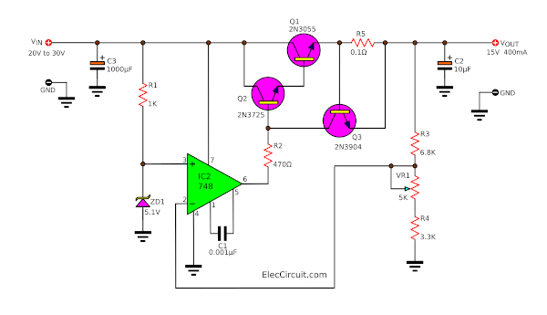
2N3055 and 748 Regulator 15V 400mA circuit


Regulator 15V 400mA by 748 and 2N3055
Today try come to see linear regulator 15volt 400mA Circuit. It is use IC op-amp IC748 perform control Voltage Regulator 15V. by have ZD1 5.1V be the referable voltage. For Transistor 2N3055 , perform enlarge current tallly go up and Q3-2N3904 help protect something through the circuit. This circuit can give Current get about 400mA only. Be regarded as the circuit experiences that interesting help give understand the system Voltage Regulator well. The detail is other , a friend has seen in the circuit please sir.
Read More

Tuesday, September 23, 2014

One Transistor FM Radio Receiver Circuit

Here’s simple FM receiver circuit for a simple superregenerative FM radio. It is sensitive, selective, and has enough audio drive for an earphone. These designs generally have low component counts, however the design or my construction have been far from simple.

FM Receiver Schematic

FM Radio Receiver Circuit Layout
Because this is a superregenerative design, component layout can be very important. The tuning capacitor, C3, has three leads. Only the outer two leads are used; the middle lead of C3 is not connected. Arrange L1 fairly close to C3, but keep it away from where your hand will be. If your hand is too close to L1 while you tune the radio, it will make tuning very difficult.

Winding L1
L1 sets the frequency of the radio, acts as the antenna, and is the primary adjustment for super-regeneration. Although it has many important jobs, it is easy to construct. Get any cylindrical object that is just under 1/2 inch (13 mm) in diameter. I used a thick pencil from my son’s grade school class, but a magic marker or large drill bit work just fine. #20 bare solid wire works the best, but any wire that holds its shape will do. Wind 6 turns tightly, side-by-side, on the cylinder, then slip the wire off. Spread the windings apart from each other so the whole coil is just under an inch (2.5 cm) long. Find the midpoint and solder a small wire for C2 there. Mount the ends of the wire on your circuit board keeping some clearance between the coil and the circuit board.

A tuning knob for C3

C3 does not come with a knob and I have not found a source. A knob is important to keep your hand away from the capacitor and coil when you tune in stations. The solution is to use a #4 nylon screw. Twist the nylon screw into the threads of the C3 tuning handle. The #4 screw is the wrong thread pitch and will jam (bind) in the threads. This is what you want to happen. Tighten the screw just enough so it stays put as you tune the capacitor. The resulting arrangement works quite well.

FM Radio Receiver Circuit Adjustment
If the radio is wired correctly, there are three possible things you can hear when you turn it on: 1) a radio station, 2) a rushing noise, 3) a squeal, and 4) nothing. If you got a radio station, you are in good shape. Use another FM radio to see where you are on the FM band. You can change the tuning range of C3 by squeezing L1 or change C1. If you hear a rushing noise, you will probably be able to tune in a station.

Try the tuning control and see what you get. If you hear a squeal or hear nothing, then the circuit is oscillating too little or too much. Try spreading or compressing L1. Double check your connections. If you don’t make any progress, then you need to change R4. Replace R4 with a 20K or larger potentiometer (up to 50K). A trimmer potentiometer is best. Adjust R4 until you can reliably tune in stations. Once the circuit is working, you can remove the potentiometer, measure its value, and replace it with a fixed resistor. Some people might want to build the set from the start with a trimmer potentiometer in place (e.g., Mouser 569-72PM-25K).

Read More