Monday, November 17, 2014
Wednesday, November 12, 2014
For safety reasons, the supply voltage is tapped off from the number plate lamp (L2), because it is on even if you accidentally drive with only the parking lights on. The wire that leads to the number plate lamp usually originates at the fuse box. As the states of the outputs of IC1a and IC1b are arbitrary when power is switched on, the reset inputs are briefly set high by the combination of C1, R1 and T1 when the lights are switched on (ignition switch on). That causes both Q outputs (pins 1 and 15) to go low. IC1a and IC1b are wired in toggle mode (J and K high).
The Set inputs are tied to ground (inactive). The driver uses pushbutton switch S1 to generate a clock pulse that causes the outputs of the flip-flops to toggle. The debouncing circuit formed by C2, R4 and T2 is essential for obtaining a clean clock pulse, and thus for reliable operation of the circuit. C1 and C2 should preferably be tantalum capacitors. The Q output of IC1b directly drives LED D1 (a low-current type, and yellow according to the regulations). The Q output of IC1a energises relay Re1 via T4 and thus applies power to the rear fog lamp L1.Circuit diagram:
Free-wheeling diode D2 protects T4 against inductive voltage spikes that occur when the relay is de-energised. In older-model cars, the charging voltage of the generator or alternator is governed by a mechanical voltage regulator. These regulators are less reliable than the electronic versions used in modern cars. For that reason, a Zener diode voltage-limiter circuit (D3 and R9) is included to keep the voltage at the emitter of T3 below 15 V and thus prevent the 4027 from being destroyed by an excessively high voltage.
The supply voltage for the circuit is tapped off from the fuse box. An accessory terminal is usually present there. Check to make sure it is fed from the ignition switch. The pushbutton switch must be a momentary-contact type (not a latching type). Ensure that the pushbutton and LED have a good ground connection. Fit the LED close to the button.The following ‘Bosch codes’ are used in the schematic:
- 15 = +12 V from ignition switch
- 58K = number plate lamp
- 86 = relay coil power (+) IN
- 85 = relay coil power OUT
- 30 = relay contact (+) IN
- 87 = relay contact OUT
Sunday, November 9, 2014
Notes:
The old and omnipresent NE555 can be very good at something it was not meant for: driving relays or other loads up to 200 mA. The picture shows an example circuit: if the input level rises over 2/3 of the supply voltage - it will turn on the relay, and the relay will stay on until the level at the input drops below one third of the supply voltage.
If the relay and D1 were connected between pin 3 and ground, the relay would be activated when the input voltage drops below one third, and deactivated when the input voltage goes over two thirds of the supply voltage.
It is also a nice advantage that the input requires only about 1 uA, which is something bipolar transistors cant compete with. (This high impedance input must not be left open.) A large hysteresis makes the circuit immune to noise. The output (pin 3) can only be either high or low (voltage-wise), and it changes its state almost instantenously, regardless of the input signal shape.
The voltage drop across the NE555s output stage (at 35-100 mA) is 0.3-2.0 V, depending on the way the relay is connected and the exact current it draws. D1 is absolutely vital to the safety of the integrated circuit.Source :: http://www.zen22142.zen.co.uk/Circuits/Switching/vcs555.htm
Read More
Sunday, November 2, 2014
1993 VW Passat Engine Control Module, Automatic Control Unit, and Automatic Solenoid Electrical Wiring Diagram are shown in the following figure. It shows the connection and wiring between each parts and component of Engine Control Module, Automatic Control Unit, and Automatic Solenoid system of the vehicle such as the multi-function switch, fuse/relay panel, knock sensor, coolant temperature sensor, shift lock solenoid, starter interlock/back up lit relay,automatic control computer clutch shut off relay, automatic control unit, automatic solenoids, program switch, throttle position sensor, full throttle switch, idle switch, throttle valve potentiometer, ignition booster, distributor firing order, engine control module, carbon canister, cold starter, idle air control valve, evap emission on/off valve, and many more. Read More
Saturday, November 1, 2014
A new image from the new phone Motorola Moto X + 1 has been filtered to show a little news that could have the cell phone.
The image comes courtesy of Evleaks shows the version of Moto X + 1 would come to Verizon in the United States. The image would confirm what we have known earlier about the new Android phone from Motorola.
Mainly, two speakers may be seen in the front, one on top and one screen in the lower part thereof. Similarly, one can see a class of sensors on each side of each of the speakers. It is not currently known that could make these sensors, but it may be related to features that do not require you to touch the screen directly to open certain applications or the like.
Additionally, one can see in the rear chamber with a larger lens and a flash on the right edge and one on the left edge of the lens. Similarly, we can see that Motorola would keep philosophy of providing a rear wood top and possibly others that allow you to customize your phone.
Although the Moto X, the previous version of this cell was characterized by very few unnecessary applications bring the operator, the photo shows the Verizon messaging application, meaning that it is expected to be the default application for this functionality in this new Motorola phone.
Wednesday, October 29, 2014
| Police Lights Circuit Schematic |
Tuesday, October 28, 2014
R1 and C1 components can be a variable type . By modifying values of R1 and C1 will vary the tone .
For this audio oscillator circuit you can use almost any transistor . To power this audio oscillator you’ll need to use a 9 volt battery or a 9 volt DC power supply .

Sunday, October 26, 2014
In this respect the relay shown has specifications of 3.5 and 1.5 V respectively, yet the circuit allows it to operate from an intermediate supply voltage of 2.5 V. Table 1 compares the relay’s power dissipation with fixed operating voltages across it, and with the circuit shown here in place. The power savings are significant. When SW1 is closed, current flows through the relay coil, and C1 and C2 begin to charge. The relay remains inactive because the supply voltage is less than its pickup voltage. The RC time constants are such that C1 charges almost completely before the voltage across C2 reaches the logic threshold of the analogue switch inside the MAX4624 IC.
When C2 reaches that threshold, the on-chip switch connects C1 in series with the 2.5 V supply and the relay coil. This action causes the relay to be turned on because its coil voltage is then raised to 5 V, i.e., twice the supply voltage. As C1 discharges through the coil, the coil voltage drops back to 2.5 V minus the drop across D1. However, the relay remains on because the resultant voltage is still above the dropout level (1.5 V). Component values for this circuit depend on the relay characteristics and the supply voltage. The value of R1, which protects the analogue switch from the initial current surge through C1, should be sufficiently small to allow C1 to charge rapidly, but large enough to prevent the surge current from exceeding the specified peak current for the analogue switch.
The switch’s peak current (U1) is 400 mA, and the peak surge current is IPEAK = (VIN – VD1) / R1 + RON) where RON is the on-resistance of the analogue switch (typically 1.2 Ω). The value of C1 will depend on the relay characteristics and on the difference between VIN and the pickup voltage. Relays that need more turn-on time requires larger values for C1. The values for R2 and C2 are selected to allow C1 to charge almost completely before C2’s voltage reaches the logic threshold of the analogue switch. In this case, the time constant R2C2 is about seven times C1(R1 + RON). Larger time constants increase the delay between switch closure and relay activation. The switches in the MAX4624 are described as ‘guaranteed break before make’. The opposite function, ‘make-before break’ is available from the MAX4625. The full datasheets of these interesting ICs may be found at http://pdfserv.maxim-ic.com/arpdf/MAX4624-MAX4625.pdf
Saturday, October 25, 2014
The requisite high voltage is generated with the aid of a small mains transformer, whose secondary winding is here used as the primary. This winding, in conjunction with C2, forms a resonant circuit. Capacitor C3 is charged to the supply voltage (12 V) via R3.When a pulse output by IC1b triggers the thyristor, the capacitor is discharged via the secondary winding. The energy stored in the capacitor is, however, not lost, but is stored in the magnetic field produced by the transformer when current flows through it. When the capacitor is discharged, the current ceases, whereupon the magnetic field collapses. This induces a counter e.m.f. in the transformer winding which opposes the voltage earlier applied to the transformer.
Circuit diagram:
This means that the direction of the current remains the same. However, capacitor C2 is now charged in the opposite sense, so that the potential across it is negative. When the magnetic field of the transformer has returned the stored energy to the capacitor, the direction of the current reverses, and the negatively charged capacitor is discharged via D1 and the secondary winding of the transformer. As soon as the capacitor begins to be discharged, there is no current through the thyristor, which therefore switches off. When C2 is discharged further, diode D1 is reverse-biased, so that the current loop to the transformer is broken, whereupon the capacitor is charged to 12 V again via R3. At the next pulse from IC1b, this process repeats itself.
Since the transformer after each discharge of the capacitor at its primary induces not only a primary, but also a secondary voltage, each triggering of the thyristor causes two closely spaced voltage pulses of opposite polarity. These induced voltages at the secondary, that is, the 230 V, winding, of the transformer are, owing to the higher turns ratio, much higher than those at the primary side and may reach several hundred volts. However, since the energy stored in capacitor C2 is relatively small (the current drain is only about 2 mA), the output voltage cannot harm man or animal. It is sufficient, however, to cause a clearly discernible muscle convulsion.
Copyright: Elektor Electronics
Thursday, October 23, 2014
| 5.1 Speaker Setup |
Accoustic Field Generator
Acoustic Field Generator is generating acoustic sound with surround effects are adjustable with a standard Dolby Surround, able to produce surround sound is good enough but not too much need of funds. Technological developments as if not only focused on one area alone but on all fronts. The development of technologies that exist today one of them is in the field of audio. With more advanced audio technology today not only as mere entertainment but has become a hobby, hobby is not cheap of course. Many audio enthusiasts trying to make music sound that sounded to be very hard to make music sound as live, the addition of the amplifier, woofer or special speakers that cost is not cheap.
The sound effects are living seems to now is something that most do not have to exist in every good audio devices. This effect is basically a surround effect that can lead to sound as though coming from different directions and his voice can still be heard clearly. Currently Compo-tape tape that has been a lot of these facilities surround sound but not good enough when heard from a considerable distance because of the effects surroundnya missing. This is because the distance is too far listener and speaker, speaker layout is not quite right, or the effect of unfavorable surround.
Surround effects are nice and can be heard with a good surround system is a system that is in movie theaters and to make it not a bit prangkat needed funds. However, if satisfaction remains the number one then the fund is not a major problem. To find a middle ground between price and quality surround effects it was attempted to make the Acoustic Field Generator that can produce surround sound is good enough but not too much need of funds. Acoustic Field Generator is capable of generating acoustic sound with surround effects are adjustable with a standard Dolby Surround.
Accoustic Field Generator Construction
Basically an Acoustic Field Generator built from op-amp circuit and filters. Op-amps are usually used as a voltage amplifier in the Acoustic Field Generator is more widely used as active filters. The filter in the tool is very instrumental in creating an acoustic sound that is really clear, but in practice, almost all the filters, do not miss the precision of the signal with a specific frequency. An op-amp is good for this application is the op-amp which has a wide bandwidth, rise time, slew rate and fast setting timenya. In addition to op-amp and active filter, theres more important parts of the power supply. This is the part that is instrumental in creating excellence acoustic sound because of the bad power supply which is the only producer of noise, which will enter into a voice signal path so that should clear acoustic sound into an acoustic sound with the addition of reverberation (noise). The power supply used is the twin power supply + / - 18 volts DC. Part Acoustic Field Generators
Before we start doing this project, it helps us know in advance about the function of each speaker.
Channel Front is a forward channel input signal LR. LR signal is passed to an amplifier with gain = 1 so that this signal is passed without change / to filter the input signal LR. Front Left and Front Right, is a public speaker that we encountered in stereo amplifier, consisting of a woofer and tweeter. Woofers generally produce low tone sound with a frequency range ranging from 80Hz - 250Hz, while the tweeter produces a high tone with a frequency range between 15kHz - 20kHz. For projects that we will create, its good we use a good quality woofer, with a size of 10 inches and a type piezoelectric tweeter for each speaker fronts.
| Front Channel 5.1 Amplifier |
Center Channel
Center, the fullrange speakers, which produce sound with a frequency range between 80Hz - 10Khz. Output from the center speaker is a summation of left and right signal (left + right = center). In a movie or song Dolby Surround format, commonly used center for dialogue / vocal or speech of the actor / artist of a film and to produce a sound that moves ahead of us.
| Center Channel 5.1 Amplifier |
Rear Channel with Surround System
| Rear Channel 5.1 Amplifier |
| Subwoofer Channel 5.1 Amplifier |
| Wiring Diagram Home Theater Amplifier / 5.1 Amplifier |
Saturday, October 18, 2014
Circuit diagram:
Here a type P521 optocoupler detects whether the fog lamp of the caravan or trailer is connected. If the fog lamp is switched on in the car, a current flows through the caravan fog lamp via diodes D1 and D2. This causes the LED in the optocoupler to light up, with the result that the photo-transistor conducts and energies the relay via transistor T1. The relay switches of the fog lamp of the car. For anyone who’s not all thumbs, this small circuit can easily be built on a small piece of perforated circuit board and then fitted somewhere close to the rear lamp fitting of the pulling vehicle.
Elektor Electronics 2008
Thursday, October 16, 2014

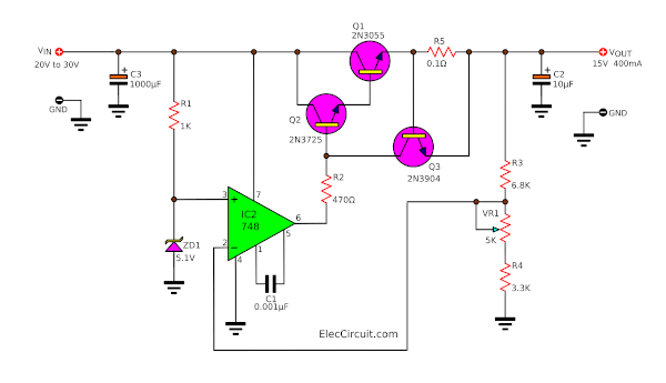
Regulator 15V 400mA by 748 and 2N3055
Today try come to see linear regulator 15volt 400mA Circuit. It is use IC op-amp IC748 perform control Voltage Regulator 15V. by have ZD1 5.1V be the referable voltage. For Transistor 2N3055 , perform enlarge current tallly go up and Q3-2N3904 help protect something through the circuit. This circuit can give Current get about 400mA only. Be regarded as the circuit experiences that interesting help give understand the system Voltage Regulator well. The detail is other , a friend has seen in the circuit please sir. Read More
Monday, October 13, 2014

Part list for 20 Ampere regulatable power supply:
- 2 x 15 volt 20+- amps
- D1…D4= Bridge rectifier MB2504 (25 amps cooled)
or eight BYW29 8 amp diodes (TO220 pinning cooled)
or 8 x MR750 (MR7510) diodes (MR750 = 6 Ampere diode) or 16 x 1N5401 (1N5408) diodes. - F1 = 2 Amp
- F2 = 25 amp
- R1 2k2 2,5 Watt
- R2 240 ohm
- R3,R4,R5,R6 0.1 ohm 10 watt
- R7 6k8
- R8 10k
- R9 47 Ohm 1 watt
- S2 mini switch
- R10 8k2
- C1,C7,C9 47nF
- C2 four times 4700uF/50v or one 22000uF/50v
- C3,C5 10uF/50v
- C4,C6,C9 100nF
- C8 330uF/50v
- C10 1uF/16v
- D5 1N4151
- D6 1N5401
- D10 MR750
- D11 LED
- D7, D8, D9 1N4001
- IC1 LM317
- Two 2N3055 transistors
- P1 5k
- P3 10k trimmer
- relay = 30 volts AC, 2×10 amp switching
S2 switches between +- 3 Amps and full output current
The relay is used to switch off the power supply voltage when the mains (S1) are/is switched off. So no delay do to the discharge of C2, and so preventing output voltages from not return to zero immediately.
A MB2504 is used as it is a 25 ampere rectifier bridge which also should be cooled. Or you could use eight BYW29 8 amp diodes (TO220 pinning) mounted on a heat sink.
Mount a little heatsink on the LM317 IC
Remember to isolate the 2N3055 transistors from the chassis/radiator! Use a radiator (heat sink) of appropriate size and surface area; insulating and heat-conducting spacer or at least a thin mica; hot adhesive and thermal paste.
Sunday, October 5, 2014
RF Oscilator Basic Explnation and Circuit

You can experiment with the size of the coil and the number of turns to see how it affects frequency and signal output of the oscillator. And the next stage is to try changing the transistor type.
You should be able to pick up its signal with a standard fm radio receiver. The "signal in" should be coupled with a disc capacitor of about 0.1 uf to the stage in front of it.
Tuesday, September 23, 2014
Here’s simple FM receiver circuit for a simple superregenerative FM radio. It is sensitive, selective, and has enough audio drive for an earphone. These designs generally have low component counts, however the design or my construction have been far from simple.

FM Receiver Schematic
FM Radio Receiver Circuit Layout
Because this is a superregenerative design, component layout can be very important. The tuning capacitor, C3, has three leads. Only the outer two leads are used; the middle lead of C3 is not connected. Arrange L1 fairly close to C3, but keep it away from where your hand will be. If your hand is too close to L1 while you tune the radio, it will make tuning very difficult.
Winding L1
L1 sets the frequency of the radio, acts as the antenna, and is the primary adjustment for super-regeneration. Although it has many important jobs, it is easy to construct. Get any cylindrical object that is just under 1/2 inch (13 mm) in diameter. I used a thick pencil from my son’s grade school class, but a magic marker or large drill bit work just fine. #20 bare solid wire works the best, but any wire that holds its shape will do. Wind 6 turns tightly, side-by-side, on the cylinder, then slip the wire off. Spread the windings apart from each other so the whole coil is just under an inch (2.5 cm) long. Find the midpoint and solder a small wire for C2 there. Mount the ends of the wire on your circuit board keeping some clearance between the coil and the circuit board.
A tuning knob for C3
C3 does not come with a knob and I have not found a source. A knob is important to keep your hand away from the capacitor and coil when you tune in stations. The solution is to use a #4 nylon screw. Twist the nylon screw into the threads of the C3 tuning handle. The #4 screw is the wrong thread pitch and will jam (bind) in the threads. This is what you want to happen. Tighten the screw just enough so it stays put as you tune the capacitor. The resulting arrangement works quite well.
FM Radio Receiver Circuit Adjustment
If the radio is wired correctly, there are three possible things you can hear when you turn it on: 1) a radio station, 2) a rushing noise, 3) a squeal, and 4) nothing. If you got a radio station, you are in good shape. Use another FM radio to see where you are on the FM band. You can change the tuning range of C3 by squeezing L1 or change C1. If you hear a rushing noise, you will probably be able to tune in a station.
Try the tuning control and see what you get. If you hear a squeal or hear nothing, then the circuit is oscillating too little or too much. Try spreading or compressing L1. Double check your connections. If you don’t make any progress, then you need to change R4. Replace R4 with a 20K or larger potentiometer (up to 50K). A trimmer potentiometer is best. Adjust R4 until you can reliably tune in stations. Once the circuit is working, you can remove the potentiometer, measure its value, and replace it with a fixed resistor. Some people might want to build the set from the start with a trimmer potentiometer in place (e.g., Mouser 569-72PM-25K).
Read MoreThe circuit in Figure 1 will give us 10 amps (12 amps surge) with performance that equals or exceeds any commercial unit. The circuit even has a current limiting feature which is a more reliable system than most commercial units have. Just like other commercial units, this circuit uses the LM723 IC which gives us excellent voltage regulation. The circuit uses 3 pass transistors which must be heat sinked. Resistor R9 allows the fine tuning of the voltage to exactly 13.8 volts and the resistor network formed by resistors R4 through R7 controls the current limiting. The LM723 limits the current when the voltage drop across R5 approaches .7 volts. To reduce costs, most commercial units rely on the HFE of the pass transistors to determine the current limiting. The fault in that system is that the HFE of the pass transistors actually increases when the transistors heat up and risks a thermal runaway condition causing a possible failure of the pass transistors. Because this circuit samples the collector current of the pass transistors, thermal runaway is not a problem in this circuit making it a much more reliable power supply. The only adjustment required is setting R9 to the desired output voltage of anywhere between 10 and 14 volts. You may use a front panel mounted 1K potentiometer for this purpose if desired. Resistor R1 only enhances temperature stability and can be eliminated if desired by connecting pins 5 and 6 of IC-1 together. Although it really isn’t needed due to the type of current limiting circuit used, over voltage protection can be added to the circuit by connecting the circuit of Figure 2 to Vout. The only way over voltage could occur is if transistors Q2 or Q3 were to fail with a collector to emitter short. Although collector to emitter shorts do happen, it is more much more likely that the transistors will open up when they fail.
Circuit diagram
I actually tested this and purposely destroyed several 2N3055’s by shorting the emitters to ground. In all cases the transistors opened up and no collector to emitter short occurred in any transistor. In any event, the optional circuit in Figure 2 will give you that extra peace of mind when a very expensive radio is used with the power supply. The circuit in Figure 2 senses when the voltage exceeds 15 volts and causes the zener diode to conduct. When the zener diode conducts, the gate of the SCR is turned on and causes the SCR to short which blows the 15 amp fuse and shuts off the output voltage. A 2N6399 (Tech America) was used for the SCR in the prototype but any suitable SCR can be used. While over voltage protection is a good idea, it should not be considered a substitute for large heat sinks. I personally feel the best protection from over voltage is the use of large heat sinks and a reliable current limiting circuit. Be sure to use large heat sinks along with heat sink grease for the 2N3055 transistors. I have used this power supply in my shack for several months on all kinds of transceivers from HF, VHF to UHF with excellent results and absolutely no hum. This power supply will be a welcome addition to your shack and will greatly enhance your knowledge of power supplies.
DE N1HFX
Parts
R1 1.5K ¼ Watt Resistor (optional, tie pins 6 & 5 of IC1 together if not used.)
R2,R3 0.1 Ohm 10 Watt Resistor (Tech America 900-1002)
R4 270 Ohm ¼ Watt Resistor
R5 680 Ohm ¼ Watt Resistor
R6,R7 0.15 Ohm 10 Watt Resistor (Tech America 900-1006)
R8 2.7K ¼ Watt Resistor
R9 1K Trimmer Potentiometer (RS271-280)
R10 3.3K ¼ Watt Resistor
C1,C2,C3,C4 4700 Microfarad Electrolytic Capacitor 35 Volt (observe polarity)
C5 100 Picofarad Ceramic Disk Capacitor
C6 1000 Microfarad Electrolytic Capacitor 25 Volt (observe polarity)
IC1 LM723 (RS276-1740) Voltage Regulator IC. Socket is recommended.
Q1 TIP3055T (RS276-2020) NPN Transistor (TO-220 Heat Sink Required)
Q2,Q3 2N3055 (RS276-2041) NPN Transistor (Large TO-3 Heat Sink Required)
S1 Any SPST Toggle Switch
F1 3 Amp Fast Blow Fuse
D1-D4 Full Wave Bridge Rectifier (RS276-1185)
T1 18 Volt, 10 Amp Transformer Hammond #165S18 (Tech America 900-5825)
author: N1HFX
e-mail:
web site: http://www.electronics-lab.com
Monday, September 22, 2014
This circuit is a simple form of the commercial UPS, the circuit provides a constant regulated 5 Volt output and an unregulated 12 Volt supply. In the event of electrical supply line failure the battery takes over, with no spikes on the regulated supply.
Circuit diagram
Notes:
This circuit can be adapted for other regulated and unregulated voltages by using different regulators and batteries. For a 15 Volt regulated supply use two 12 Volt batteries in series and a 7815 regulator. There is a lot of flexibility in this circuit.
TR1 has a primary matched to the local electrical supply which is 240 Volts in the UK. The secondary winding should be rated at least 12 Volts at 2 amp, but can be higher, for example 15 Volts. FS1 is a slow blow type and protects against short circuits on the output, or indeed a faulty cell in a rechargeable battery. LED 1 will light ONLY when the electricity supply is present, with a power failure the LED will go out and output voltage is maintained by the battery. The circuit below simulates a working circuit with mains power applied:
Between terminals VP1 and VP3 the nominal unregulated supply is available and a 5 Volt regulated supply between VP1 and VP2. Resistor R1 and D1 are the charging path for battery B1. D1 and D3 prevent LED1 being illuminated under power fail conditions. The battery is designed to be trickle charged, charging current defined as :-
(VP5 - 0.6 ) / R1
where VP5 is the unregulated DC power supply voltage.
D2 must be included in the circuit, without D2 the battery would charge from the full supply voltage without current limit, which would cause damage and overheating of some rechargeable batteries. An electrical power outage is simulated below:
Note that in all cases the 5 Volt regulated supply is maintained constantly, whilst the unregulated supply will vary a few volts.
Standby Capacity
The ability to maintain the regulated supply with no electrical supply depends on the load taken from the UPS and also the Ampere hour capacity of the battery. If you were using a 7A/h 12 Volt battery and load from the 5 Volt regulator was 0.5 Amp (and no load from the unregulated supply) then the regulated supply would be maintained for around 14 hours. Greater A/h capacity batteries would provide a longer standby time, and vice versa.
author: Andy Collinson
e-mail: anc@mitedu.freeserve.co.uk
web site: http://www.zen22142.zen.co.uk
Monday, September 15, 2014