Showing posts with label switch. Show all posts

Friday, November 14, 2014

SWITCH DEBOUNCING CIRCUIT

Switch debouncing is one of those things you generally have to live with when playing with switches and digital circuits. If you want to input a manual switch signal into a digital circuit youll need to debounce the signal so a single press doesnt appear like multiple presses. This circuit will remove the transient spikes and contact bounces from a non-latching push button switch.

Circuit Diagram


Notes

Using a 555 timer as a monostable circuit, it is easy to build a good switch debouncer circuit. There are many circuits for SPDT debouncing, but not many for a normally open, push-to-make press button switch (PBS). The 555 monostable gives an output pulse of around 20 ms with component values shown. The formula for determining the output pulse is:

Tout = 1.1 R1 C1

With the values in my circuit this equates to :

Tout = 1.1*1.8*106*10*10-9 = 0.0198 sec or 19.8 ms

The 555 circuit can be re-triggered if the input is held low longer than the output pulse. To prevent this happening, I have included a further timing circuit comprised of the 1Meg resistor and 47n capacitor. Normally, the 47n capacitor is discharged via the 1 Meg resistor. When the switch is pressed the capacitor quickly charges and provides a brief negative pulse to the 555 input. When the capacitor is fully charged, the potential across the voltage divider formed by the 10k and 1Meg resistors is insufficient to retrigger the monostable. Releasing the switch quickly discharges the capacitor. The output of a 555 monostable is suitable for connecting to TTL and CMOS logic circuits.
Read More

Sunday, November 9, 2014

Voltage Controlled Switch using 555 Timer descroption and circuit


Notes:
The old and omnipresent NE555 can be very good at something it was not meant for: driving relays or other loads up to 200 mA. The picture shows an example circuit: if the input level rises over 2/3 of the supply voltage - it will turn on the relay, and the relay will stay on until the level at the input drops below one third of the supply voltage.

If the relay and D1 were connected between pin 3 and ground, the relay would be activated when the input voltage drops below one third, and deactivated when the input voltage goes over two thirds of the supply voltage.

It is also a nice advantage that the input requires only about 1 uA, which is something bipolar transistors cant compete with. (This high impedance input must not be left open.) A large hysteresis makes the circuit immune to noise. The output (pin 3) can only be either high or low (voltage-wise), and it changes its state almost instantenously, regardless of the input signal shape.

The voltage drop across the NE555s output stage (at 35-100 mA) is 0.3-2.0 V, depending on the way the relay is connected and the exact current it draws. D1 is absolutely vital to the safety of the integrated circuit.Source :: http://www.zen22142.zen.co.uk/Circuits/Switching/vcs555.htm
Read More

Saturday, November 8, 2014

Automatic TV Lighting Switch

The author is the happy owner of a television set with built-in Ambilight lighting in the living room. Unfortunately, the television set in  the bedroom lacks this feature. To make up for this, the author attached a small lamp to the wall to provide background lighting, This makes  watching television a good deal more enjoyable, but it ’s  not the ideal solution. Although the TV set can be  switched off with the remote  control, you still have to get out of bed to switch off the lamp.

Circuit diagram :

Automatic TV Lighting Switch Circuit Diagram

Consequently, the author devised this automatic lighting switch that switches the background light on and off along with the T V set. The entire circuit is fitted in series with the mains cable of the TV set, so there’s no need to tinker with the set. It works as follows: R1 senses  the current drawn by the TV  set. It has a maximum value  of 50 mA in standby mode,  rising  to around   500 m A  when  the  set  is  operating. The voltage across R1 is limited by D5 during negative  half- cycles  and  by  D1– D4  during positive half-cycles.  T he  voltage  across  these  four diodes charges capacitor C1 via D6 during positive  half-cycles. This voltage drives the internal LED of solid-state switch TRI1 via R2, which causes the internal triac to conduct and pass the mains voltage to the lamp.   Diode D7 is not absolutely necessary, but  it is recommended because the LED in the  solid-state switch is not especially robust  and cannot handle reverse polarisation. Fuse  F1 protects the solid-state switch against  overloads. T he  value  of  use d  here  (10 Ω)  for  resistor R1 works nicely with an 82-cm (32 inch)  LCD screen.

With smaller sets having lower  power consumption, the value of R1 can be  increased to 22 or 33 Ω, in which case you  should use a 3-watt type. Avoid using an  excessively high resistance, as otherwise TRI1 will switch on when the TV set is in standby mode.  Some TV sets have a half-wave rectifier in the  power supply, which places an unbalanced  load on the AC power outlet. If the set only  draws current on negative half-cycles, the cir-cuit won’t work properly. In countries with  reversible AC power plugs you can correct  the problem by simply reversing the plug. Compared with normal triacs, optically cou-pled solid-state relays have poor resistance  to high switch-on currents (inrush currents).

For this reason, you should be careful with  older-model TV sets with picture tubes (due  to demagnetisation circuits). If the relay fails,  it usually fails shorted, with the result that the TV background light remains on all the time. If you build this circuit on a piece of perf-board, you must remove all the copper next  to conductors and components carrying  mains voltage. Use PCB terminal blocks with a spacing of 7.5 mm. This way the separation between the connections on the solder  side will also be 3 mm. If you fit the entire  arrangement as a Class II device, all parts of  the circuit at mains potential must have a  separation of at least 6 mm from any metal  enclosure or electrically conductive exterior  parts that can be touched.
Read More

Friday, September 26, 2014

Automatic Day Night Twilight Switch Circuit

 Here is a circuit which will automaticaily light your porch light or activate any other device when the ambient light drops below a certain level.
A ·light dependent resistor is used in series with a relay. The resistor has a value in excess of ‘l megohm when illuminated, this drops A7  to below 110 ohms when day light. It is important that the LDR be positioned in such a place as not to receive any spurious illumination as this will cause the relay to drop out intermittently. A bimetallic strip type relay will give sufficient delay to ensure that incident light flashes have no influence.

Automatic Day/Night, Twilight Switch Circuit


Read More

Wednesday, September 24, 2014

Capacitive Switch Circuit Diagram

  1. The 555 or 7555 timers will oscillate in a stable manner.
  2. However, if we add an external capacitive sensor it becomes possible to vary the oscillation frequency. In this circuit the square wave is integrated by the triple RC network, while lC2, used as a comparator (with a variable reference value), uses the changes in the integrated voltage to alternately make and break the relay. Thus when you move close to C the relay makes; if you remain stationary the relay breaks.
  3. By changing the existing frequency of the signal the average integrated value remains the same but, at the instant when the frequency is changed, a positive or negative voltage peak will appear due to the momentary change in the average waveform of the signal.
  4. Failing this the operation of the circuit would often be disrupted by false detections. Coarse l and fine adjustment is provided, using P1 and P2, to reduce the risk of incorrect switching. Note: The numbers in parentheses are the pins if an LM3l1 is used in place of the CA3130.
  5. Without this refinement the size of the sensitive plate must be such that the frequency of oscillation be at least , several kHz.
  6. It may seem a bit basic but it is a valid idea and it is worth ) looking at it in greater detail.
  7. Take a square wave signal with a given frequency and integrate it. This gives a stable continuous average voltage.
  8. To obtain better results you could take the signal after integration and differentiate between negative pulses (the frequency decreases as the value of C increases: when the sensor is approached) and positive pulses (the frequency increases again if the sensor is no longer affected) and compare them.
  9. This is the principle upon which our switch is based. 
Capacitive Switch Circuit Diagram

Read More

Friday, September 19, 2014

A Headphone Monitoring Switch

In any recording situation, monitoring is critical to make sure youre getting what you want on tape. This is just as true in field recording, but in most cases, ones monitoring options are severely limited--stereo headphone is the only choice.

Headphone Monitoring Switch  :

A

Since I often use dual-mono mics, hearing a stereo feed of the two is not always convenient. I wanted the option to hear JUST the left mic in BOTH ears, or just the right mic in both ears, as well as a normal stereo signal. This is simple enough to do with a big rotary switch. When completed, you can create a little box that your headphones plug into, which in turn is plugged into the stereo phone output of your deck. Then, by turning the knob on the switch box, you can hear normal stereo, left-only mono, right-only mono, left+right mono and even left-right reversed stereo (or normal stereo again). 

Note the use of summing resistors in the left+right mono section. This was an attempt to prevent the two outputs from "fighting" each other if there were very different voltages in left and right outputs. I used 8 ohm resistors here, but a higher value might be better. Maybe ~20 ohms? Also, I initially decided to put normal stereo on both ends of the switchs travel so Id always be able to find it without looking. However, I sometimes wish to have left-right reversed. If youd like to try this, simply swap the leads on one of the "normal stereo" connections. 

One final caveat: The left only/right-only mono positions are -6dB down, since only one half of the decks headphone amp is driving your phones when the switch is in those positions. 


Source by : Ediagramlab
Read More

Saturday, September 6, 2014

Using Cd4066B Touch Switch Wiring diagram Schematic

Build a Using Cd4066B Touch Switch Circuit Diagram.The CD4066B consists of four bilateral switches, each with independent controls. When touch switch SI is activated, R4 is driven high, and the control voltage goes high, which latches the switch. When S2 is activated, R4 goes low and the control voltage goes low, which deactivates the switch.

Using Cd4066B Touch Switch Circuit Diagram


Using

Read More

Thursday, September 4, 2014

Battery Switch With Low Dropout Regulator Wiring diagram Schematic

This is a simple Battery Switch With Low-Dropout Regulator Circuit Diagram. In the form of the LT1579 Linear Technology (www.linear-tech.com) has produced a practical battery switch with an integrated low-dropout regulator. In contrast to previous devices no diodes are required. The schema is available in a 3.3 V version (LT1579CS8-3.3) and in a 5 V version (LT1579CS8-5), both in SO8 SMD packages. There is also an adjustable version and versions in an SO16 package which offer a greater range of control and drive signals. The main battery, whose terminal voltage must be at least 0.4 V higher than the desired output voltage, is connected to pin IN1. The backup battery is connected to pin IN2. The regulated output OUT can deliver a current of up to 300 mA. The LDO regulator part of the IC includes a pass transistor for the main input voltage IN1 and another for the backup battery on IN2.


Battery_Switch_With_LDO_Regulator_Circuit_Diagramw

The IC will switch over to the backup battery when it detects that the pass transistor for the main voltage input is in danger of no longer being able to maintain the required output voltage. The device then smoothly switches over to the backup battery. The open-drain status output BACKUP goes low to indicate when this has occurred. When neither battery is able to maintain the output voltage at the desired level the open-drain output DROPOUT goes low. The LT1579 can operate with input voltages of up to +20 V from the batteries. The regulator output OUT is short-schema proof. The shutdown input switches off the output; if this feature is not required, the input can simply be left open.


Streampowers
Read More

Monday, September 1, 2014

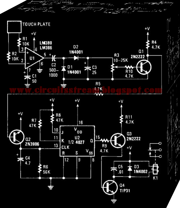
Electronic Touch Switch 1 Wiring diagram Schematic

This is an Electronic Touch Switch 1 Circuit Diagram. This switch reacts to the touch of a finger to turn lights and/or appliances on or off. The device uses the human body as an antenna to pick up 60-Hz hum, which is applied to a metal plate by your finger. The signal is fed to the input of Ul, an LM380 audio-power amplifier. An LM386 should work as well. 
 

 Electronic Touch Switch 1 Circuit Diagram


 electronic touch switch 1 circuit diagram
 
The 60-Hz output from the amplifier is rectified by Dl and D2, then filtered by C3. Potentiometer R3 sets the trigger voltage used to saturate Ql. When Ql turns on, the collector end of R4 goes almost to ground and provides the needed voltage to turn on Q2. Transistor Q2 turns on and clocks. 
 
The flip-flop is configured for toggle-mode operation, so its output switches states with each clock pulse. The 4027 (U2) is wired to toggle by tying the J and inputs high and the set and resets low. Transistor Q3 is connected to the Q output through the 4.7-KOhmhm resistor. Transistor Q3 drives Q4, the relay driver. Be sure that the load does not exceed the relay ratings.
Read More

Sunday, August 31, 2014

Long Delay Stop Switch

Long-Delay Stop Switch Circuit Diagram. Presettable times for train stops in stations are indispensable if you want to operate your model railway more or less realistically according to a timetable. This schema shows how a 555 timer can be used with a relatively small timing capacitor to generate very long delay times as necessary by using a little trick (scarcely known among model railway electronic technicians): pulsed charging of the timing net-work. Such long delays can be used in hidden yards with through tracks, for instance.  As the timer is designed for half-wave operation, it requires only a single lead to the transformer and one to the switching track or reed contact when used with a Märklin AC system (H0 or H1). The other lead can be connected to any desired grounding point for the common ground of the track and lighting diagram.

Long-Delay
Long-Delay Stop Switch Circuit Diagram

As seen from the outside, the timer acts as a monostable flip-flop. The output (pin 3) is low in the quiescent state. If a negative signal is applied to the trigger input (pin 2), the output goes high and C4 starts charging via R3 and R4. When the voltage on C4 reaches 2/3 of the supply voltage, it discharges via an internal transistor connected to pin 7 to 1/3 of the supply voltage and the output (pin 3) goes low. The two threshold values (1/3 and 2/3) are directly proportional to the supply voltage. The duration of the output signal is independent of the supply voltage: t= 1.1(R4 + R5) × C4 

if the potentiometer is connected directly to the supply line (A and B joined). The maximum delay time that can be generated using the component values shown in the schematic diagram is 4.8 minutes. How-ever, it can be increased by a factor of approximately 10 if the timing network is charged using positive half-waves of the AC supply voltage (reduced to the 10–16-V level) instead of a constant DC voltage. 

The positive half-waves of the AC voltage reach the timing network via D2, the transistor, and D3. Diode D3 prevents C4 from being discharged between the pulses. The total resistance of R4 and R5 should not be too high (no more than 10 MΩ if possible), since electrolytic capacitors (such as are needed for C4) have significant leakage currents. Incidentally, the leakage current of aluminium electrolytic capacitors can be consider-ably reduced by using a supply voltage well below the rated voltage. Capacitor C6 is intended to suppress noise. It forms a filter network in combination with an internal voltage-divider resistor.
If a vehicle happens to remain standing over the reed switch so the magnet holds the contacts constantly closed, the timer will automatically be retriggered when the preset delay times out. In this case the relay armature will not release and the locomotive will come to the ‘end of the line’ in violation of the timetable. This problem can be reliably eliminated using R6, R7 and C5. This trigger schema ensures that only one trigger pulse is generated, regardless of how long the reed switch remains closed. RC network R8/C7 on the reset pin ensures that the timer behaves properly on switch-on (which is far from being something to be taken for granted with many versions of the 555 or 556 dual timer).
Reed switches have several special characteristics that must be kept in mind when fitting them. The contact blades, which are made from a ferromagnetic material, assume opposite magnetic polarities under the influence of a magnetic field and attract each other. Here the position and orientation of the magnet, the distance between the magnet and the reed switch, and the direction of motion of the magnet relative to the switch are important factors. The fragility of the glass hous-ing and the thermal stress from soldering (stay at least 3 mm away from the glass housing) require a heat sink to be used between the soldering point and the glass/metal seal. A suitable tweezers or flat-jawed pliers can be used for this pur-pose. If you need to bend the leads, use flat-jawed pliers to protect the glass/metal seal against mechanical stresses. 

Matching magnets in various sizes are available from toy merchants and electronics mail-order firms. They should preferably be fitted underneath the loco-motive or carriage. However, the magnet can also be fitted on the side of a vehicle with a plastic body. In this case the reed switch can be hidden in a mast, bridge column or similar structure or placed in a tunnel, since the distance must be kept to less than around 10 mm, even with a strong magnet. If fitting the schema still presents problems (especially with Märklin Z-gauge Mini-Club), one remedy is to generate the trigger using a unipolar digital Hall switch, such as the Siemens TLE4905L or Allegro UGN3120. To avoid coupled-in interference, the stop timer should be fitted relatively close to the Hall sensor (use screened cable if necessary). Pay attention to the polarity of the magnet when fitting it to the bottom of the vehicle. With both types of sensors, the South pole must point toward the front face of the Hall IC (the face with the type marking). The North pole is sometimes marked by a dab of paint. Generally speaking, the polarity must be determined experimentally. 

Fitting the schema is not a problem with Z-gauge and 1-gauge tracks, since the distance between the iron parts (rails) and the Hall switch is sufficiently large. In an HO system, some modifications must be made to the track bed of the Märklin metal track. Cut a suitably sized ‘window’ between one wheel rail and the centre rail in order to prevent secondary magnetic diagram from interfering with the operation of the sensor. Keep the distance between the magnet and the case of the Hall switch between 5 and 10 mm, depending on the strength of the magnet, to ensure reliable actuation.
Read More

On Off Touch Switch Circuit

The modern mechanic switches are improved concerning of old technology. We need however many times to replacement some old switch or to check currents bigger than the durability of certain switches or simple we need something with modern appearance. For he and different reasons is essential the up schema. It is simple in the manufacture and the materials that use they exist everywhere.


Parts:

R1 = 3.3M
R2 = 3.3M
R3 = 10K
R4 = 1K
C1 = 10nF-63V
D1 = 1N4007
D2 = Red LED
Q1 = BC547
IC1 = NE555
RL1 = 12V Relay


This schema is based on the well known timer IC 555 (IC1), which drives a relay of which the contacts play the role of switch. The metal surfaces can have what form we want, but it should they are clean and near in the schema. In order to it changes situation it suffices touch soft somebody from the two plates. Plate MP1 in order to the contacts of RL1 close [ON], or plate MP2 in order to the contacts of RL1 open [OFF]. The current that RL1 will check depended from his contacts. The Led D2 turns on when the switch they are in place ON and the contacts of RL1 closed. Two small pieces of metal can be used instead of MP1 – MP2. Because MP = Metal Plate.

Read More

Wednesday, August 20, 2014

Automatic Soldering Iron Switch Wiring diagram Schematic

Quite often, we forget to turn off the soldering iron. This results in not only a smoking oxidised iron but also waste of electricity. To solve this problem, here’s a schema that automatically switches off the soldering iron after a predetermined time. The schema draws no power when it is inactive. The schema can also be used for controlling the electric iron, kitchen timer or other appliances.

Automatic Soldering Iron Switch Circuit Diagram

Automatic


At the heart of the schema is a monostable multivibrator built around timer IC 555. When the schema is in sleep mode, to switch on the soldering iron, you should push switch S1 momentarily. The multivibrator gets triggered and its output pin 3 goes high for around 18 minutes to keep relay RL1 energised via transistor T1. At the same time, capacitor C3 charges and AC supply is provided to switch on the soldering iron via normally opened (N/O) contacts of relay RL1.

The soldering iron remains ‘on’ for the time period predetermined by resistor R1 and capacitor C2. Here, this time is set for 18 minutes. Flashing of LED1 indicates the heating progress of the soldering iron. When the predetermined time is over, relay RL1 de-energises to turn off the soldering iron and the buzzer sounds until capacitor C3 gets discharged.

For switching on the schema, use either a bell push switch or a similar switch with appropriate current carrying capacity.


Sourced By: EFY Author  T.A. Babu
Read More

Simple Audio Controlled Switch Wiring diagram Schematic

This is a Simple Audio Controlled Switch Circuit Diagram. The audio-controlled switch combines a pair of 741 op amps, two 2N2222 general-purpose transistors, a hexFET, and a few support components to a schema that can be used to turn on a tape recorder, a transmitter, or just about anything that uses sound.

Simple Audio Controlled Switch Circuit Diagram


Read More