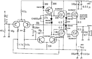
Amplilfier power series from the beginning until now did not experience any changes. Some say this series is good, but the series was good fitting assembly and tested the results are not as we expected.
The problem is usually treble is less subtle, less sound, sound breaking, buzz, middle of the field tested the bass sound is lost. so you do not have to believe what people 100%. The quality amplifier built-up would differ greatly with the amplifier assembly, a series can be the same but the quality will depend on who manufacture it.
Here are a few tricks to try
How to cope with a buzzing sound
Power amplifiers are often used in the field blazer. This circuit is said said person is a bell assembly. But you do not immediately interested in this power, the circuit rather complicated and difficult to understand reflect the intelligence of people who first mendisainnya. In my opinion a great power is the power of simple, inexpensive, easily assembled and rational. You do not need to use expensive components such as the price of tantalum capacitors, power mosfet and the other expensive. This does not determine the quality of the power amp so that we raft. Power of sometimes causing buzzing, to overcome that is by holding the line input jack ground to the ground with 10-22 ohm resistors. So do not just take the ground input from the ground but held first with the R 10 ohms.
How to setting bias trimpot
Rotate the trimpot bias (if any) until the drain current of 50-100mA on each power transistor, in order to avoid defects treble in volume in the top position at 10. The risks are so panassss heatsink! (This setting marks on plate A-AB)
Offset trimpot setting
At the time of input without a signal, turn the trimpot so that the voltage on the speaker offsets actually read 0 volts. If you do not want to bother, use and entrust it with ic type series from Hitachi HA17741 IC brand quality or other! This is the heart of the series, 90-95% of quality is determined from the IC circuit this!
Overcoming the voice
Use pre-amp circuit to increase the signal of at least 2 times. normally and should pre-amp circuit uses IC op-amps with +12 V minimum supply-12V. Raise his mid tone!
If hard you do not want to just use the tone control circuit IC is his mid!
The secret is not in his mid tone alone, but the signal output from the IC op-amps are usually large.
Treble rupture
Excessive treble will damage the power amp, power rather than out even ngedrop. Handle, attach the filter capacitor on the input 1NF power amp to ground to ensure the signal is not disabled. Always use a quality active components such as ICs and transistors, 500 price difference will also be different results.
Use a large cable and short as possible, especially for leg power transistor, and this transistor should be directly soldered to the pcb.
Missing bass in field
Usually power for field use supplay CT 50V 50V transformer, or at least 42V 42V ct. The greater the greater the supply voltage watt channeled though the series is written only 300-400 Watts only. This course uses Elko capacitors with voltage 80-100V. 10.000uF/100V capacitor will be equal to 4X10.000uF/50V and of course voltage capacitor is filled with full / almost full.
Try to use a strong Elko at temperatures of 105 C. Capacitors are strong in supply of more than nominal voltage is written on his body. For example 4700uF/50V 85C capacitor will quickly explode in voltage 51V 85C. And Elko will be strong 105C 4700uF/50V voltage supplied more than 50V at a temperature of 85C. Elco so that it does not quickly explode if given the full voltage, keep its temperature as cold as possible, fan with the cool air.
For speaker
Try using a driver speakers that have a large spool diameter fitted with a suitable size bok. Usually included examples of the parameters / dimensions bok. Size bok bok2 usually larger than that sold in the market. if you force using bok that from this market, use driver type G12-80 (sorry no fear brand called promotion) speakers with bass tones to wall size small. Bok wall should be thick, strong and do not forget glued! Bok who will not be glued with a different sound, especially bass tones, prove it!
Heat Sensor
The form of transistor, the transistor is usually type BD139 MJE340 or it could be located in the center, flanked by a pair of transistors having a certain equal. These transistors must be mounted on the main heatsink to detect the heat generated by power transistors. It acts to lower bias currents at the hot heatsink. So what heatsink and power transistors must be set diposisi hot? Yes objectives nothing to prevent the signal from the defect (in class A or AB), with consequent heat. This class is not necessary and will not be felt if you only want the bass tones only. Goal setting on. AB grade is still crystal clear sound even though the maximum volume positioned rotated (in the middle of the field).
It is unlikely, but its closer.
Large heatsink
Not only electrolytic capacitors are more explosive at high temperatures, power transistors can also break away under stress break the original. For example 2SC5200 transistors have the break voltage of 230Vdc, but if temperaturya high voltage values will break his fall well below this value, resulting in faster transistor is damaged. Use of heatsink and cooling fan is very important not only to reduce the heat, more than it can prevent the transistor from break / damaged and weakened output. Increasingly hot temperatures will be more or less ability. Use of this cooling is expected for the components remain fresh, fit and durability.
Choice Component
Power Transistor
There are so many types and models of these transistors, for example MJ15003 MJ15024-4 and-5 from Motorola, but unfortunately these components are not manufactured by Motorola again but from ON semiconductor. Transistor model jengkol usually stronger in the high temperature, probably due to more airtight. 2SC5200 from Toshiba, this transistor is equal dalamannya Sanken 2SC2922 Korea, and both will break if the temperature is too hot. 2SC2922 Sanken issued tin granules when heated, this weakness, the Japanese technology is better than Korean technology. 2SC3281, this transistor is the most popular and frequently used in professional amplifier, but Toshiba does not produce much, if still there in the market, then it most likely is fake!
Transfomer
There are two models of the transformer which is often used, namely EI model (box / conventional) and the model toroid (ring / donut). Some say the toroid transformer model is better because it has a smaller flux leak, in fact the same. Circuits that are sensitive to this flux is high berpenguatan circuits like pre-amp head and mic pre-amp. The circuit is usually installed horizontally / flat parallel to the structure of a conventional transformer wire so that a series of emails received reverberation is greater. Unlike the model toroid transformer is arranged in a vertical wire their email so that the wires are perpendicular to circuit kits The effect is the flux of the pre-amp kit receive a smaller head. To solve for this flux does not enter the series is by downloading shelding / fortified with non-magnetic plate such as aluminum plate and copper plate / sheet pcb board. Plate is of course connected to ground via a cable. To match the flux in a vertical transmission, the conventional transformer needs to be installed side (the side be side down) so that the arrangement of transformer wire stand upright, this method is often used in built-up POWER2. Voltage 50V 50V CT can be obtained by combining the two transformer 25VCT25V, CT is not used, the foot 25V 50V so that the legs be made only to CT, bringing the total number is 100V or 50VCT50V. It deserves used for pwr amp powerless over 400Watt.
Resistor 5 Watt
Resistor on the power transistor legs are usually valued at 0.5 ohm 5 Watt white square. If we dismantle dalamannya it appears there was a circular aluminum wire. It resembles the inductor, the inductive reactance inductor will be higher when fed a high-frequency fractions so that treble tone will be weakened and deformed. Power required to remove the high notes (treble) of course greater, there is a problem here. The use of R 0.5/5W on its home-based power amplifier ok-ok only. But often do not realize the cause of damage to the speakers and power amplifiers is the high treble tones. Treble is not out but was hit by a pwr amp so arising is hot and damaged. We recommend using common Watt resistor 2 12:47 - 1 ohm parallel 2 so that counted 4 Watt. Or if you use 0:22 ohm 2 Watt Resitor unnecessary because the voltage clamp diparalel quite half (one R 0.5/5W replaced one R 0.22/2W) its ok.
Fuse
Nature damage to semiconductor materials / transistor power amplifier is short, if you use a supply that is high enough then the destruction of these transistors will invite their partners to be damaged as well. In order for the destruction of this transitor congregation not need the installation of fuses. 1.5A per power transistor is considered sufficient.



 or 8
or 8


