Showing posts with label circuit. Show all posts

Tuesday, January 6, 2015

Audio Stereo Power Amp Circuit

audio-power-amp-schematic

This is a 50 Watt Audio power amplifier circuit based single IC STK4036II. Use heatsink to prevent overheating on the IC. 

The amplifier circuit will give you good quality of sound unexpensive and have low price. 

It is easy we make a power amplifier using only few external components. 

The STK4036II amplifier are will find in enough eponymous stereo amplifiers , but also in enough activety loudspeakers. 
Read More

Friday, December 12, 2014

Phone ringtone generator circuit


ringtone-generator-schematic
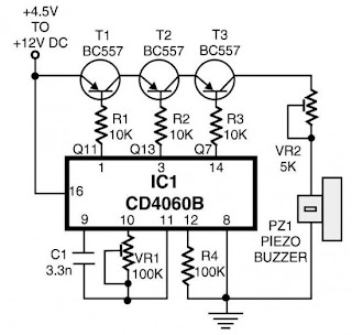
This is a simple home telephone ringtone generator circuit which is built with applying only several electronic components / parts.It generates simulated telephone ringtone and requires only DC supply with 4.5V DC to 12V DC voltage.One may possibly use this circuit in ordinary intercom or phone-type intercom. 

The sound is pretty loud when this circuit is operated on +12V DC power supply. Even so, the volume of ring sound can be adjusted.
Read More

Thursday, December 11, 2014

Variable Power Supply Circuit

0-28v
This is the schematic diagram of variable power supply.The output voltage of this power supply circuit can be adjust from 0V to 28V DC, while the current output is static the rang is about 6A up to 8A.
Read More

Thursday, November 20, 2014

IC555 Tester Circuit Diagram


555 timer tester is a simple circuit that serves to test the condition of IC 555. 555 timer circuit tester, in principle, start the timer 555 in astable multivibrator mode. As an indicator of the status of the timer 555 good condition or damaged to use 2 pieces LED which will light up in a blink alternately when the timer 555 in good condition. And only one will turn on or off all the timer 555 when the condition is broken. 555 timer circuit tester is powered using 9 Volt DC voltage source.

How to use 555 timer tester is in conjuction with IC 555 to test the existing IC socket according to the order button. Then activate the power switch to begin testing the 555 timer ic. Then live we observe the LED indicators 2buah before, whether flashing alternately (good) or not blink or even die all (timer 555 damaged).
Read More

Wednesday, November 19, 2014

Rain Detector Circuit

Rain Detector Using 555 is a simple alarm that can be used to find out when rain was came. Rain Detector Using In principle this is an a stable multivibrator 555 which is prepared by IC555 with a sensor attached that can detect water. A stable multivibrator with the 555 is set in the audio frequency with a frequency of 1 KHz. Rain Detector circuit 555 can be supply with voltage source that is free enough from 5-15 VDC.


Circuit Rain Detector can be mounted on motorcycle, car or other object that we want to protect from rain. Water sensor used in the circuit  Rain Detector Using IC 555.  We can make with a PCB that we make the path as shown in the image above by using aluminum foil  board or insulator boards.
Read More

1 5V Amplified Ear Circuit Diagram

1.5V1.5V Amplified Ear Circuit Diagram

Device purpose:

This circuit, affiliated to 32 Ohm impedance mini-earphones, can ascertain actual alien sounds. Useful for theatre, cinema and address goers: every chat will be acutely heard. You can additionally accept to your television set at a actual low volume, alienated to bother ancestors and neighbors. Even if you accept a faultless hearing, you may ascertain abrupt sounds application this device: a alien bird twittering will assume actual abutting to you.

Circuit operation:

The affection of the ambit is a constant-volume ascendancy amplifier. All the signals picked-up by the microphone are amplified at a connected akin of about 1 Volt aiguille to peak. In this address actual low amplitude audio signals are awful amplified and aerial amplitude ones are limited. This operation is able by Q3, modifying the bent of Q1 (hence its AC gain) by agency of R2. A noteworthy affection of this ambit is 1.5V array operation. Typical accepted drawing: 7.5mA.

Notes:

  • Due to the constant-volume control, some users may consider P1 volume control unnecessary. In most cases it can be omitted, connecting C6 to C3. In this case use a SPST slider or toggle switch as SW1.
  • Please note the stereo output Jack socket (J1) connections: only the two inner connections are used, leaving open the external one. In this way the two earpieces are wired in series, allowing mono operation and optimum load impedance to Q4 (64 Ohm).
  • Using suitable miniature components, this circuit can be enclosed in a very small box, provided by a clip and hanged on ones clothes or slipped into a pocket.
  • Gary Pechon from Canada reported that the Amplified Ear is so sensitive that he can hear a whisper 7 meters across the room.
    He hooked a small relay coil to the input and was able to locate power lines in his wall. He was also able to hear the neighbors stereo perfectly: he could pick up the signals sent to the speaker voice coil through a plaster wall.
    Gary suggests that this circuit could make also a good electronic stethoscope.
Read More

SAMSUNG protect circuit with LA76931

Following is the protect circuit Samsung TV which use IC LA76931 as basic working the protect circuit. This Protect Circuit LA76891 located at pin-30 whichconnected to the collector of transistor Q902.In normal conditions the voltage at the base of Q902 is "low" and the voltage at pin-30 is "high". For the temporary crippling protect, it can be removed Q902 (or to the emitter-base short).

SAMSUNG protect circuit with LA76931
Sampling circuit protect from:

Vertical Protect. Pulses of the vertical-out rectified by diode D355, so that the base voltage is approximately 0.6V Q904 ,and collector voltage is 0v.
X-ray Protect (option). Sampled using a heater voltage of the circuit as shown below. Normal vltage in x-ray path to the base of Q902 is zero.

ABL protect. If there is damage to flyback voltage which can cause a high rise ABL, then protect circuit will actively work.
Read More

Tuesday, November 18, 2014

Protectors Circuit on SMPS power supply

The simplest example SMPS which still uses 3 transistors (C3807, A1015 and power transistors) classic problem that often occurs is: - Problem in the feedback circuit can cause the output voltage B + over so that it can endanger the aircraft as a whole. For example elco erupted, pcb burnt burnt by over-heated, horizontal transistor short.

- Problem on feedback circuits may cause power regulator transistor is damaged due to over current transistor (eg, due to the 47k resistor transistor circuit on the secondary error detector value is delayed).
- If the input ac voltage drops can cause the power regulator transistor is damaged, due to over current transistor If the secondary there is a power transistor short can cause damage over current regulator.
- Protectors are designed to make the SMPS SMPS "reliable will not be damaged" if there are things that go wrong as mentioned above. 

SMPS Circuit

SMPS circuit using IC systems generally are designed with a surge protector, which include:
  • Over voltage protector (OVP)
  • Over current protector (OCP)
  • Over load protector
  • Short circuit protector
  • Over temperature protector
Read More

Schematic Audio Amplifier Circuit 200W

Output Power : 200Watts
Load Resistance : 8ohms
Input impedance : 55K
Maximum supply voltage : (+95v)-0-(-95v)
Recommended supply voltage : (+66v)-0-(-66v)

This complete aerial quality, low babble address audio ability amplifier is based about the Hybrid Integrated Ambit STK4050 bogus by Sanyo. The ambit incorporates aggregate and has a best music achievement ability of 200W.The ambit incorporates an on lath ability supply; therefore, alone centre broke agent is appropriate to ability the circuit. I t has actual acceptable affection sound. U can use it with your Home Theatre your PC & etc... You can additionally use it as Subwoofer Amplifier.

It is a bunched amalgamation for THIN-TYPE Audio sets. Easy Heatsink architecture to banish calefaction generated in THIN-TYPE audio sets. Constant-Current ambit to Reduce accumulation switch-ON and switch-OFF shock noise. External accumulation switch-On and switch-OFF shock babble muting, Load circumlocute protection, thermal abeyance and added circuits can be tailored-designed.
Read More

Monday, November 17, 2014

Zero Crossing Detector Circuit

Zero Crossing Detector circuit is basically an application of a comparator. In the article series Zero Crossing Detector with Op Amp is built using a comparator of an Op Amp IC741/351. The process of detection of this comparator is  0Volt input signal crossing point by making reference value at comparator 0Volt.


 The output of the Zero Crossing Detector circuit with Op Amp is wave-shaped box that detection result of the crossroads of 0 volt input signal.
Read More

Tips and Tricks on Audio Power Amplifier Circuit

Amplilfier power series from the beginning until now did not experience any changes. Some say this series is good, but the series was good fitting assembly and tested the results are not as we expected.
The problem is usually treble is less subtle, less sound, sound breaking, buzz, middle of the field tested the bass sound is lost. so you do not have to believe what people 100%. The quality amplifier built-up would differ greatly with the amplifier assembly, a series can be the same but the quality will depend on who manufacture it.

Here are a few tricks to try

How to cope with a buzzing sound
Power amplifiers are often used in the field blazer. This circuit is said said person is a bell assembly. But you do not immediately interested in this power, the circuit rather complicated and difficult to understand reflect the intelligence of people who first mendisainnya. In my opinion a great power is the power of simple, inexpensive, easily assembled and rational. You do not need to use expensive components such as the price of tantalum capacitors, power mosfet and the other expensive. This does not determine the quality of the power amp so that we raft. Power of sometimes causing buzzing, to overcome that is by holding the line input jack ground to the ground with 10-22 ohm resistors. So do not just take the ground input from the ground but held first with the R 10 ohms.


How to setting bias trimpot
Rotate the trimpot bias (if any) until the drain current of 50-100mA on each power transistor, in order to avoid defects treble in volume in the top position at 10. The risks are so panassss heatsink! (This setting marks on plate A-AB)

Offset trimpot setting
At the time of input without a signal, turn the trimpot so that the voltage on the speaker offsets actually read 0 volts. If you do not want to bother, use and entrust it with ic type series from Hitachi HA17741 IC brand quality or other! This is the heart of the series, 90-95% of quality is determined from the IC circuit this!

Overcoming the voice
Use pre-amp circuit to increase the signal of at least 2 times. normally and should pre-amp circuit uses IC op-amps with +12 V minimum supply-12V. Raise his mid tone!
If hard you do not want to just use the tone control circuit IC is his mid!
The secret is not in his mid tone alone, but the signal output from the IC op-amps are usually large.

Treble rupture
Excessive treble will damage the power amp, power rather than out even ngedrop. Handle, attach the filter capacitor on the input 1NF power amp to ground to ensure the signal is not disabled. Always use a quality active components such as ICs and transistors, 500 price difference will also be different results.
Use a large cable and short as possible, especially for leg power transistor, and this transistor should be directly soldered to the pcb.

Missing bass in field
Usually power for field use supplay CT 50V 50V transformer, or at least 42V 42V ct. The greater the greater the supply voltage watt channeled though the series is written only 300-400 Watts only. This course uses Elko capacitors with voltage 80-100V. 10.000uF/100V capacitor will be equal to 4X10.000uF/50V and of course voltage capacitor is filled with full / almost full.
Try to use a strong Elko at temperatures of 105 C. Capacitors are strong in supply of more than nominal voltage is written on his body. For example 4700uF/50V 85C capacitor will quickly explode in voltage 51V 85C. And Elko will be strong 105C 4700uF/50V voltage supplied more than 50V at a temperature of 85C. Elco so that it does not quickly explode if given the full voltage, keep its temperature as cold as possible, fan with the cool air.

For speaker
Try using a driver speakers that have a large spool diameter fitted with a suitable size bok. Usually included examples of the parameters / dimensions bok. Size bok bok2 usually larger than that sold in the market. if you force using bok that from this market, use driver type G12-80 (sorry no fear brand called promotion) speakers with bass tones to wall size small. Bok wall should be thick, strong and do not forget glued! Bok who will not be glued with a different sound, especially bass tones, prove it!

Heat Sensor
The form of transistor, the transistor is usually type BD139 MJE340 or it could be located in the center, flanked by a pair of transistors having a certain equal. These transistors must be mounted on the main heatsink to detect the heat generated by power transistors. It acts to lower bias currents at the hot heatsink. So what heatsink and power transistors must be set diposisi hot? Yes objectives nothing to prevent the signal from the defect (in class A or AB), with consequent heat. This class is not necessary and will not be felt if you only want the bass tones only. Goal setting on. AB grade is still crystal clear sound even though the maximum volume positioned rotated (in the middle of the field).
It is unlikely, but its closer.

Large heatsink
Not only electrolytic capacitors are more explosive at high temperatures, power transistors can also break away under stress break the original. For example 2SC5200 transistors have the break voltage of 230Vdc, but if temperaturya high voltage values ​​will break his fall well below this value, resulting in faster transistor is damaged. Use of heatsink and cooling fan is very important not only to reduce the heat, more than it can prevent the transistor from break / damaged and weakened output. Increasingly hot temperatures will be more or less ability. Use of this cooling is expected for the components remain fresh, fit and durability.


Choice Component
Power Transistor
There are so many types and models of these transistors, for example MJ15003 MJ15024-4 and-5 from Motorola, but unfortunately these components are not manufactured by Motorola again but from ON semiconductor. Transistor model jengkol usually stronger in the high temperature, probably due to more airtight. 2SC5200 from Toshiba, this transistor is equal dalamannya Sanken 2SC2922 Korea, and both will break if the temperature is too hot. 2SC2922 Sanken issued tin granules when heated, this weakness, the Japanese technology is better than Korean technology. 2SC3281, this transistor is the most popular and frequently used in professional amplifier, but Toshiba does not produce much, if still there in the market, then it most likely is fake!

Transfomer
There are two models of the transformer which is often used, namely EI model (box / conventional) and the model toroid (ring / donut). Some say the toroid transformer model is better because it has a smaller flux leak, in fact the same. Circuits that are sensitive to this flux is high berpenguatan circuits like pre-amp head and mic pre-amp. The circuit is usually installed horizontally / flat parallel to the structure of a conventional transformer wire so that a series of emails received reverberation is greater. Unlike the model toroid transformer is arranged in a vertical wire their email so that the wires are perpendicular to circuit kits The effect is the flux of the pre-amp kit receive a smaller head. To solve for this flux does not enter the series is by downloading shelding / fortified with non-magnetic plate such as aluminum plate and copper plate / sheet pcb board. Plate is of course connected to ground via a cable. To match the flux in a vertical transmission, the conventional transformer needs to be installed side (the side be side down) so that the arrangement of transformer wire stand upright, this method is often used in built-up POWER2. Voltage 50V 50V CT can be obtained by combining the two transformer 25VCT25V, CT is not used, the foot 25V 50V so that the legs be made only to CT, bringing the total number is 100V or 50VCT50V. It deserves used for pwr amp powerless over 400Watt.

Resistor 5 Watt
Resistor on the power transistor legs are usually valued at 0.5 ohm 5 Watt white square. If we dismantle dalamannya it appears there was a circular aluminum wire. It resembles the inductor, the inductive reactance inductor will be higher when fed a high-frequency fractions so that treble tone will be weakened and deformed. Power required to remove the high notes (treble) of course greater, there is a problem here. The use of R 0.5/5W on its home-based power amplifier ok-ok only. But often do not realize the cause of damage to the speakers and power amplifiers is the high treble tones. Treble is not out but was hit by a pwr amp so arising is hot and damaged. We recommend using common Watt resistor 2 12:47 - 1 ohm parallel 2 so that counted 4 Watt. Or if you use 0:22 ohm 2 Watt Resitor unnecessary because the voltage clamp diparalel quite half (one R 0.5/5W replaced one R 0.22/2W) its ok.

Fuse
Nature damage to semiconductor materials / transistor power amplifier is short, if you use a supply that is high enough then the destruction of these transistors will invite their partners to be damaged as well. In order for the destruction of this transitor congregation not need the installation of fuses. 1.5A per power transistor is considered sufficient. 
Read More

Sunday, November 16, 2014

Digital Volume Control Circuit using MAX5486

A channel digital volume circuit on IC MAX5486 is shown here. MAX5486 40K digital volume / balance controller that pushbutton interface. The IC bias voltage that eliminated of an external circuitry for purpose and thereby by reduces external count. The IC has an LED indicator driver circuit be used for driving the indicator LEDs indicates level and balance level. The IC operated from or power and in pin TSSOP package. circuit on MAX5486 applied applications like personal audio systems, audio devices, home theatre systems, audio systems, audio systems etc.

The right channel input is applied to the pin8 (high terminal (HR) of internal digital potentiometer of the IC) and left channel input is applied to the pin17 (high terminal (HL) of the second internal digital potentiometer of the IC). Low terminals (pin and 6) of potentiometers are shorted and connected to the mid bias voltage output (pin11) of the IC. at the buffered wiper terminal (pin10) of internal potentiometer and left channel output at the buffered wiper terminal of the second internal potentiometer of the IC. A 1uF capacitor is connected from the bias generator bypass (pin12) to ground. of this capacitor is noise bypassing. of capacitors C4 and C5 are to bypass noise from the VDD and VLOGIC sources. This improves stability and performance of the circuit.

LEDs D1 to D5 are the indicator LEDs indicates volume and balance levels. R1 to R5 limits current through the corresponding LEDs. 1M resistor R6 for activating the indicator LED drivers. LED D6 represents operation mode of IC. When it glows, the IC is in balance mode and when off, the IC in volume mode. Resistor R7 limits through LED D6. volume mode the LEDs work a bar graph indicating volume. balance mode, the centremost LED alone glows when a centred balance. mute mode, all indicator LEDs OFF.

Push button switches S1 to S4 are used for controlling the circuit. Pressing S1 push the IC into mute mode. Push button S4 used between volume mode and balance mode and LED D6 indicated it. Push button S2 and S3 are used for increasing and decreasing volume mode and shifting the balance to left and right balance mode. The Vss pin of the IC is grounded single operation circuit. Shutdown pin (pin6) is tied to the VLOGIC for disabling the shutdown . Connecting the shutdown pin to drive the IC to the shutdown mode.

The output of the MAX5486 is sufficient enough to drive high impedance headphones. For driving low impedance headphones or speakers an amplifier stage be added to the output. power dissipation of MAX5486 is 675mW and consider this point while selecting the loads.
Read More

Friday, November 14, 2014

SWITCH DEBOUNCING CIRCUIT

Switch debouncing is one of those things you generally have to live with when playing with switches and digital circuits. If you want to input a manual switch signal into a digital circuit youll need to debounce the signal so a single press doesnt appear like multiple presses. This circuit will remove the transient spikes and contact bounces from a non-latching push button switch.

Circuit Diagram


Notes

Using a 555 timer as a monostable circuit, it is easy to build a good switch debouncer circuit. There are many circuits for SPDT debouncing, but not many for a normally open, push-to-make press button switch (PBS). The 555 monostable gives an output pulse of around 20 ms with component values shown. The formula for determining the output pulse is:

Tout = 1.1 R1 C1

With the values in my circuit this equates to :

Tout = 1.1*1.8*106*10*10-9 = 0.0198 sec or 19.8 ms

The 555 circuit can be re-triggered if the input is held low longer than the output pulse. To prevent this happening, I have included a further timing circuit comprised of the 1Meg resistor and 47n capacitor. Normally, the 47n capacitor is discharged via the 1 Meg resistor. When the switch is pressed the capacitor quickly charges and provides a brief negative pulse to the 555 input. When the capacitor is fully charged, the potential across the voltage divider formed by the 10k and 1Meg resistors is insufficient to retrigger the monostable. Releasing the switch quickly discharges the capacitor. The output of a 555 monostable is suitable for connecting to TTL and CMOS logic circuits.
Read More

Thursday, November 13, 2014

741 op amp bassed Alarm project electronic circuit with explanation


A very simple alarm project electronic circuit can be designed using a common 741 operational amplifier IC and some other common electronic parts . As you can see in the schematic circuit , this alarm project is activated by some normal open contacts , connected in parallel . If one of those contact is closed the alarm will sound .
This alarm project is composed from an audio frequency generator , a small audio amplifier stage and a small command stage .

The audio frequency generator is designed using a 741 operational amplifier ( or some other similar type ) .The T2 and T2 transistors forms a small audio amplifier and the normal opened contacts I1to I3 forms the command stage ( you can use how many contacts you need ).
In stand-by mode when all contacts are opened T1 transistor is locked and the alarm is inactive . If one of the contact is closed T1 transistor will activate the relay that will activate alarm . One the alarm starts to sound it can not be stopped until the I contact will be opened ( the circuit will be unplugged from the power source) .

The relay used in this project must have a 12 volts nominal voltage ( 10 volts activation) with a maximum working current of 10-30mA.
This circuit project must be powered from a 12 volt DC power supply .

Read More

Fluorescent Light Wiring Diagram Tube Light Circuit

This post "Fluorescent Light Wiring Diagram | Tube Light Circuit" is about how to wiring fluorescent light and "how a Fluorescent Tube Light works". The wiring process of fluorescent tube lamp/light with Ballast,Starter is quite easy and simple. In most cases when we buy a fluorescent light it comes in a complete set with all wire connected. If you want do it yourself (DIY), you can buy all the parts individually. And you can complete all connection of the fluorescent light/lamp with the help of this wiring circuit diagram.

Fluorescent Light Wiring Diagram


Fig:Fluorescent Light Wiring Diagram

Main parts of Fluorescent Tube Light:

     1.Fluorescent Tube
     2.Ballast
     3.Starter
     4.Holder, wire etc.

How Fluorescent Lights works:

The starter is like a key of fluorescent light because it is used to light up the tube. When we connect the AC supply voltage to the circuit, then the starter act like short circuited and current flow through those filament (located at the first and second end of the tube light) and the filament generate heat and it ionized the gas (mercury vapor) in the fluorescent tube lamp. So the gas becomes electrically conductive medium. At the same time when the starter opened the circuit path of two filaments from series connected, then the ballast release its stored voltage. And it makes the fluorescent tube fully lighten. Now the starter has no job in the circuit, if you open it from the circuit the fluorescent tube light will be still lighten, until you release the main supply. 
Read More

LB1948M bassed forward reverse motor control driver circuit with explanation


A very simple forward reverse motor control driver electronic circuit project can be designed using the LB1948M 2 channel low saturation voltage forward reverse motor control driver IC. LB1948M motor driver is optimal for motor drive in 12V system products and can drive either two DC motors, one DC motor using parallel connection, or a 2-phase bipolar stepping motor with 1-2 phase excitation mode drive.
Some features of the LB1948M motor driver IC are : 12V power supply ,low saturation voltage: VO(sat) = 0.5V (typical) at IO = 400mA ,zero current drawn in standby mode , braking function ,built-in thermal shutdown circuit .

The LB1948M can be used as a single-channel H-bridge power supply by connecting IN1 to IN3, IN2 to IN4, OUT1 to OUT3, and OUT2 to OUT4 as shown in the figure. (IOmax=1.6A, VO(sat)=0.6V (typical) at IO=800mA) .
The circuit is very simple and require few external electronic parts .

Read More

TDA1562 bassed One IC 50W Audio Amplifier circuit

The integrated output amplifier described in this article consists of little more than one integrated circuit. It is intended especially for use in motor vehicles and other battery-operated applications. Although it appears simple and hardly worth looking at, the amplifier can produce an appreciable audio power output. The circuit diagram in Figure 2 emphasizes how few external components are needed to construct a complete output amplifier.

One-IC 50W Audio Power Amplifier Using TDA1562 circuit project

For instance, the new device does not need compensation networks to enhance the stability. Also, because of the absence of switch-on phenomena, there is no need for a switch-on delay network. There is, of course, still a need for supply line decoupling capacitors. Capacitors C5 and C6 are required for Class-H operation, about which more in the box. The value of input capacitors C1 and C2 is relatively low, thanks to the high input impedance of the IC. Switched RC network R4-C4 at the ‘mode select’ input (pin 4) serves to switch the IC to ‘mute’ or ‘standby’.

One-IC 50W Audio Power Amplifier Using TDA1562 circuit diagram

When the supply voltage is switched on, the IC is first switched automatically to the ‘mute’ mode and to ‘on’ only after a short delay. The time constant R4-C4 is a few tenths of a second and this delay between the two states is sufficient to obviate disturbing (and annoying) switch-on phenomena. Switch S1 enables the amplifier to be switched to ‘standby when the use of the amplifier is not needed for a period of time. When that time has elapsed, the amplifier is quickly reverted to normal operation. The current drain in the standby mode is virtually negligible at only 200µA. Resistor R3 prevents a short-circuit current ensuing when S1 is being closed at the instant C4 is being discharged.

One-IC 50W Audio Power Amplifier Using TDA1562 circuit

One-IC 50W Audio Power Amplifier Using TDA1562 circuit schematic

Measurement results (at Ub=14.4 V)
Supply voltage

* 8–18 V

Sensitivity

* 760 mV r.m.s.

Input impedance

* 70 kΩ

Power output

* 54 W r.m.s. into 4 Ω (f=1 kHz; THD+N=1%)

Harmonic distortion (THD+N)

* at 1 W into 4 Ω: 0.046% (1 kHz)
* 0.29% (20 kHz)
* at 35 W into 4 Ω: 0.12% (1 kHz)
* 0.7% (20 kHz)

Signal-to-noise ratio (with 1 W into 4 Ω)

* 88 dBA

Power bandwidth

* 7.5 Hz – 185 kHz (at 25 W into 4 Ω)

Quiescent current

* about 135 mA (‘on’)

Resistors:

* R1 = 1MΩ
* R2 = 4kΩ7
* R3 = 1kΩ
* R4 = 100kΩ

Capacitors:

* C1,C2 = 470nF
* C3,C4 = 10µF 63V radial
* C5,C6,C8 = 4700µF 25V radial
* (18mm max. dia., raster 7.5 mm)
* C7 = 100nF, raster 5 mm

Semiconductors:

* D1 = high-efficiency-LED
* IC1 = TDA1562Q (Philips)

Miscellaneous:

* S1 = single-pole on/off switch
* Four spade connectors, PCB mount Heatsink for IC1 (Rth<2.5 k/w)
Read More

Wednesday, November 12, 2014

Rear Fog Lamp For Vintage Cars Diagram Circuit

According to current legislation in many countries, vintage cars must also be fitted with a fog lamp at the rear. In modern cars, there is a bit of circuitry associated with the fog lamp switch to prevent the fog lamp from going on when the lights are switched on if the driver forgot to switch it off after the last patch of fog cleared up. The circuit described here extends that technology back in time. The circuit is built around a dual JK flip-flop (type 4027). T3 acts as an emitter follower, and it only supplies power to the circuit when the lights are switched on.

For safety reasons, the supply voltage is tapped off from the number plate lamp (L2), because it is on even if you accidentally drive with only the parking lights on. The wire that leads to the number plate lamp usually originates at the fuse box. As the states of the outputs of IC1a and IC1b are arbitrary when power is switched on, the reset inputs are briefly set high by the combination of C1, R1 and T1 when the lights are switched on (ignition switch on). That causes both Q outputs (pins 1 and 15) to go low. IC1a and IC1b are wired in toggle mode (J and K high).

The Set inputs are tied to ground (inactive). The driver uses pushbutton switch S1 to generate a clock pulse that causes the outputs of the flip-flops to toggle. The debouncing circuit formed by C2, R4 and T2 is essential for obtaining a clean clock pulse, and thus for reliable operation of the circuit. C1 and C2 should preferably be tantalum capacitors. The Q output of IC1b directly drives LED D1 (a low-current type, and yellow according to the regulations). The Q output of IC1a energises relay Re1 via T4 and thus applies power to the rear fog lamp L1.Circuit diagram:
Rear Fog Lamp Circuit Diagram For Vintage Cars

Free-wheeling diode D2 protects T4 against inductive voltage spikes that occur when the relay is de-energised. In older-model cars, the charging voltage of the generator or alternator is governed by a mechanical voltage regulator. These regulators are less reliable than the electronic versions used in modern cars. For that reason, a Zener diode voltage-limiter circuit (D3 and R9) is included to keep the voltage at the emitter of T3 below 15 V and thus prevent the 4027 from being destroyed by an excessively high voltage.

The supply voltage for the circuit is tapped off from the fuse box. An accessory terminal is usually present there. Check to make sure it is fed from the ignition switch. The pushbutton switch must be a momentary-contact type (not a latching type). Ensure that the pushbutton and LED have a good ground connection. Fit the LED close to the button.The following ‘Bosch codes’ are used in the schematic:
  • 15 = +12 V from ignition switch
  • 58K = number plate lamp
  • 86 = relay coil power (+) IN
  • 85 = relay coil power OUT
  • 30 = relay contact (+) IN
  • 87 = relay contact OUT
Author: Eric Vanderseypen - Copyright: Elektor Electronics Magazine
Read More

LT3433 based Step Up Step Down DC to DC Converter Circuit Diagram circuit with explanation


The illustration provides below schemes 8V-60V to 12V Converter Circuit Diagram. It uses LT3433, an automatic step up and step down switching regulator IC with 4V to 60V input voltage which can be useful in automotive electronics using various wide input voltage range.

According to the LT3433 datasheet, this Automatic Step-Up and Step-Down Conversion device is a 200kHz fixed frequency current mode switching regulator using a single inductor which can be applied in applications such as wall adapter powered systems and battery power voltage buffering.

Read completely about Step Up/Step Down DC to DC Converter Circuit Diagram using LT3433 here in pdf archive (source: linear.com)

Read More

Tuesday, November 11, 2014

Suzuki GSX1300 Hayabusa Charging System Circuit 99 – 00

SuzukiThe circuit of Suzuki GSX1300 Hayabusa Charging System composed of generator, regulator/rectifier unit and battery. The AC current generated from the generator is rectified by the rectifier and is turned into DC current, then it charges the battery. While the engine rpm is low and the generated voltage of generator is lower then the adjusted voltage of regulator, the regulator does not function. However, the generated current charges the battery directly at this time.

When the engine rpm becomes higher, the generated voltage of the generator also becomes higher and the voltage between the battery terminals becomes high accordingly. When it reaches the adjusted voltage of the integrated circuit and it is turned “ON”, a signal will be sent to the SCR (thyristor) gate probe and the SCR will be turned “ON”. Then the SCR becomes conductive in the direction from point A to point B. At this time the current generated from the generator gets through the SCR without charging the battery and returns to generator again.

Read More